TEL:+86 132 6656 7067





The rapid growth of artificial intelligence, cloud computing, and high-performance computing is placing increasing pressure on conventional electrical interconnects. Modern data centers must transfer enormous volumes of information between processors, switches, accelerators, and storage systems. As transmission speeds increase, electrical channels face greater challenges involving signal loss, power consumption, and physical connectivity.
Integrated photonics is emerging as an important technology for addressing these limitations. By combining multiple optical functions onto compact photonic integrated circuits, it can reduce the dependence on separately packaged optical components and support higher levels of integration. Silicon photonics, heterogeneous integration, advanced optical packaging, and photonic engine development are contributing to this transition.
The impact extends beyond individual optical transceivers. Integrated photonics is influencing the development of 800G and 1.6T connectivity, near-packaged optics, co-packaged optics, and optical I/O architectures. These technologies are helping the industry rethink how optical signals are generated, modulated, transmitted, and received inside next-generation computing systems.
1. Why High-Speed Optical Interconnects Need Integrated Photonics
Electrical interconnects remain essential throughout modern computing systems, but their performance becomes increasingly difficult to scale as data rates and connection density rise. High-speed electrical signals experience attenuation, reflections, crosstalk, and frequency-dependent distortion as they travel through PCB traces, connectors, and package substrates.
These effects increase the engineering effort required to maintain signal integrity. Equalization and retiming can compensate for some channel impairments, but additional processing may increase power consumption and design complexity.
Optical transmission offers a different approach. Instead of carrying high-speed information through electrical conductors over the entire connection, optical links convert electrical data into light and transmit it through optical waveguides or fiber.
Integrated photonics helps make this approach more compact by bringing multiple optical functions onto a shared chip or integrated platform.
Several industry developments are accelerating its adoption:
Higher data rates: 800G and 1.6T interfaces require increasingly sophisticated optical and electrical components.
AI accelerator scaling: Large GPU clusters generate substantial communication traffic between processors and network devices.
Bandwidth density: Computing systems need more communication capacity within limited package and rack space.
Power efficiency: Energy consumption per transmitted bit is becoming an important system-level design metric.
Optical integration: Combining optical functions can reduce component count and support compact architectures.
Advanced packaging: Chiplet, 2.5D, and 3D integration create opportunities for closer electrical and optical integration.
2. What Is Integrated Photonics?
Integrated photonics is a technology approach that combines multiple optical functions on a common photonic chip or integrated platform. These functions may include light generation, modulation, splitting, filtering, routing, and detection.
Traditional optical systems often use separate components for different functions. An optical transmitter, for example, may contain a laser, driver, modulator, coupling elements, and other optical components. A receiver may contain a photodetector, transimpedance amplifier, and associated signal-processing circuitry.
Integrated photonics combines selected optical functions into a more compact structure. Depending on the platform and architecture, it can reduce the number of discrete optical components and simplify certain optical paths.
A photonic integrated circuit (PIC) is the core component in many integrated photonics systems. It contains optical structures fabricated on a photonic material platform, allowing light to be guided and processed through integrated waveguides and functional devices.
| Optical Function | Typical Integrated Component | Purpose |
|---|---|---|
| Light Generation | Integrated or externally coupled laser | Provides the optical carrier |
| Optical Modulation | Mach-Zehnder or ring modulator | Encodes electrical information onto light |
| Optical Routing | Waveguide and optical coupler | Directs light through the photonic circuit |
| Wavelength Management | Filters, resonators, and multiplexers | Separates or combines optical wavelengths |
| Optical Detection | Photodiode or integrated detector | Converts received light into electrical signals |
| Signal Conditioning | Associated electronic circuitry | Drives, amplifies, and processes electrical signals |
Not every integrated photonics platform contains all these functions on one chip. The final architecture depends on the material system, wavelength, transmission rate, manufacturing process, and application requirements.
3. Silicon Photonics Becomes a Major Integration Platform
Silicon photonics is one of the most important technology platforms for integrated optical communication. It uses silicon-based fabrication processes to create optical waveguides and functional photonic devices on silicon substrates or compatible silicon-based structures.
Silicon photonics benefits from the mature semiconductor manufacturing ecosystem. Established lithography, wafer processing, and packaging capabilities can support high-volume production of complex photonic circuits.
Its advantages include:
Compact optical structures: Silicon waveguides can guide light through small integrated circuit layouts.
High integration potential: Multiple optical functions can be fabricated within a common photonic platform.
Semiconductor manufacturing compatibility: Selected fabrication processes can leverage established CMOS-related manufacturing infrastructure.
Scalable circuit design: Reusable photonic building blocks support different optical architectures.
Electronic integration opportunities: Silicon photonics can be combined with electronic ICs through advanced packaging and heterogeneous integration.
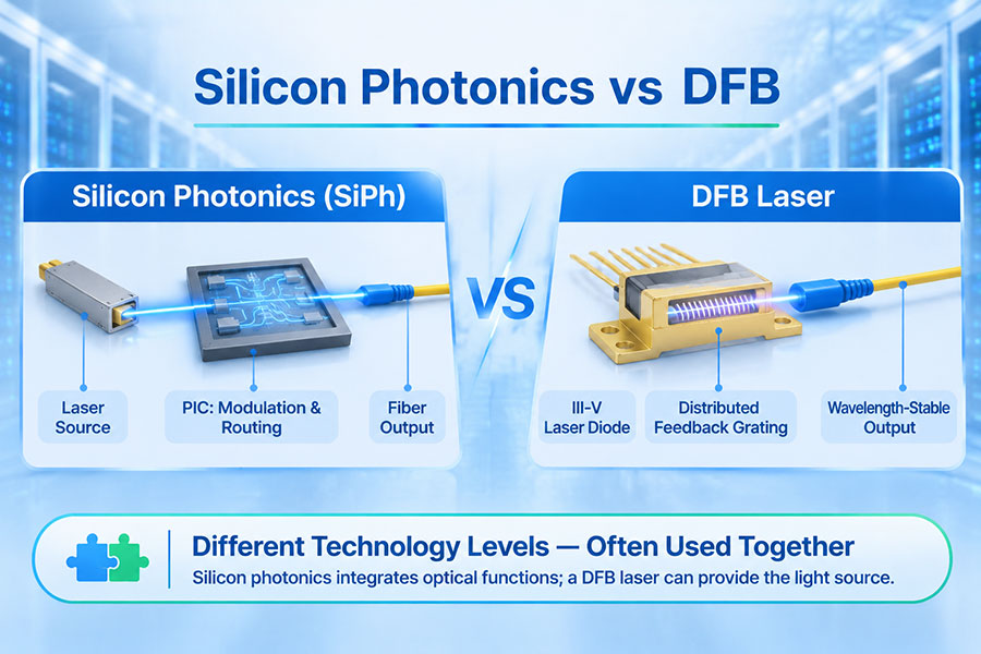
However, silicon does not efficiently generate light through conventional electrically driven laser emission. As a result, silicon photonic systems commonly use external laser sources or integrate suitable III-V semiconductor light sources through bonding or other heterogeneous integration techniques.
This distinction is important. Silicon photonics provides an effective platform for optical waveguides and many passive and active photonic functions, but a complete optical system may still require additional materials and components.
4. Photonic Integrated Circuits Combine Multiple Optical Functions
A photonic integrated circuit brings optical components together on a shared platform. Instead of connecting every optical function through separate fiber or free-space interfaces, light can travel between integrated devices through precisely designed waveguides.
A PIC used in a high-speed optical transmitter may include modulators, optical splitters, waveguides, and wavelength-management structures. A receiver PIC may integrate optical routing and detection functions, depending on the design.
Common PIC building blocks include:
Waveguides: Guide optical signals through the photonic circuit.
Modulators: Change optical properties according to the electrical data signal.
Couplers: Split or combine optical signals between waveguides.
Filters: Select or suppress specific wavelength components.
Multiplexers and demultiplexers: Combine or separate multiple wavelength channels.
Photodetectors: Convert optical signals into electrical current.
Resonators: Provide wavelength-selective optical functions in suitable designs.
Integrating these functions can reduce the number of discrete optical connections and improve the compactness of the optical engine. It also creates new requirements for precise fabrication, optical coupling, thermal control, and device characterization.
5. Heterogeneous Integration Connects Different Material Platforms
One material platform rarely provides the best performance for every photonic function. Silicon is attractive for waveguides and large-scale photonic integration, while other semiconductor materials may provide better light generation, detection, or modulation characteristics for specific applications.
Heterogeneous integration combines different materials or device technologies within one integrated system. It allows engineers to select suitable materials for individual functions rather than forcing every component onto a single platform.
Common integration approaches include:
| Integration Method | Basic Approach | Engineering Objective |
|---|---|---|
| Hybrid Integration | Combines separately fabricated optical and electronic components | Uses specialized components within a common package |
| Heterogeneous Integration | Combines different material systems through bonding or related processes | Integrates complementary material properties |
| Monolithic Integration | Fabricates multiple compatible functions on one substrate | Reduces separate component interfaces |
| 2.5D Integration | Connects multiple dies through an interposer or advanced substrate | Provides dense chip-to-chip connections |
| 3D Integration | Stacks or vertically connects different device layers | Increases integration density and shortens selected interconnects |
These methods are not interchangeable. Each involves different manufacturing processes, alignment requirements, thermal characteristics, and production economics.
Heterogeneous integration is particularly important for combining silicon photonics with III-V lasers, specialized detectors, and electronic ICs. It allows optical systems to use different material properties within a coordinated package.
6. Optical Modulators and Photodetectors Support Higher Data Rates
Optical modulators and photodetectors are fundamental components in high-speed optical interconnects. Their performance directly affects the quality of electrical-to-optical and optical-to-electrical conversion.
In a transmitter, the modulator encodes information onto an optical carrier. In a receiver, the photodetector converts the incoming optical signal into an electrical signal for subsequent processing.
Integrated photonics supports the development of compact devices that can be incorporated into high-density optical engines.
Common optical modulator technologies include:
Mach-Zehnder Modulators: Use interference between optical paths to control the output signal.
Microring Modulators: Use wavelength-sensitive resonant structures to modulate light in compact devices.
Electro-Absorption Modulators: Control optical absorption through an applied electrical signal.
Other material-specific modulators: Use different electro-optic effects according to the photonic platform.
Photodetectors are selected according to wavelength, bandwidth, sensitivity, responsivity, noise, and integration requirements. Germanium-on-silicon photodetectors are one example of a technology used in silicon photonics systems operating in relevant telecommunications wavelength bands.
At higher data rates, the bandwidth and linearity of these devices become increasingly important. Their performance must be evaluated together with the driver, receiver amplifier, DSP, and electrical interface rather than in isolation.
7. Integrated Photonics Supports 800G and 1.6T Optical Connectivity
The transition to 800G and 1.6T optical interfaces is increasing the demand for compact, high-performance optical engines. These modules must support more data while operating within strict mechanical, electrical, and thermal constraints.
Integrated photonics can help address these requirements by combining multiple optical functions and supporting high-density optical channel architectures.
| Optical Generation | Representative Architecture | Integration Considerations |
|---|---|---|
| 400G | Multiple 100G-class lanes or supported alternative configurations | Multi-channel optical integration and electrical signal conditioning |
| 800G | 8 × 100G or 4 × 200G architectures, depending on the interface | Higher optical channel density and improved packaging |
| 1.6T | 8 × 200G in common next-generation architectures | 200G-class lane performance and advanced optical-electrical integration |
| Future 3.2T | Higher aggregate bandwidth and future lane architectures | Further improvements in photonic integration, packaging, and thermal design |
Integrated photonics does not automatically determine the data rate of an optical module. The achievable performance also depends on the modulation format, lane rate, optical device bandwidth, DSP, FEC, electrical interface, and host platform.
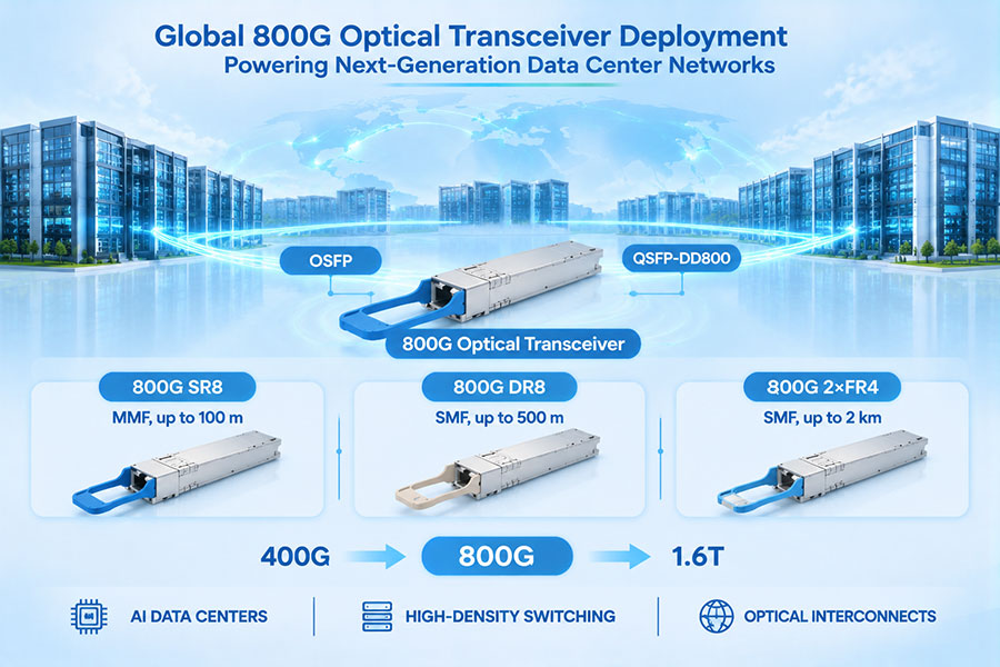
For example, an 800G module may use different lane configurations and optical technologies depending on whether it is designed for short-reach parallel transmission, single-mode connectivity, or coherent transport. The photonic integration approach must match the specific optical architecture.
8. Optical Engines Move Closer to Switching and Computing Chips
Traditional pluggable optical modules are installed at the front panel of switches and other network equipment. Electrical signals travel from the switch ASIC through the PCB and connector to the optical module, where they are converted into optical signals.
As electrical interface speeds increase, the distance between the switch ASIC and the optical engine becomes an important design consideration. Longer electrical paths can introduce additional signal loss and increase the need for equalization and retiming.
New packaging approaches seek to place optical engines closer to the computing or switching silicon.
These approaches include:
Pluggable Optics: Optical transceivers are installed in standardized front-panel cages and can be replaced independently.
Linear Pluggable Optics: Uses a simplified electrical architecture in compatible systems to reduce selected signal-processing functions.
Near-Packaged Optics: Places optical engines close to the main ASIC while retaining a degree of physical separation.
Co-Packaged Optics: Integrates optical engines within the same package environment as the switch ASIC or other high-performance silicon.
Optical I/O: Uses optical interfaces to connect computing components and systems where electrical interconnect limitations become significant.
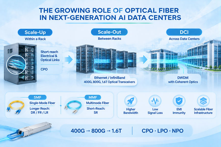
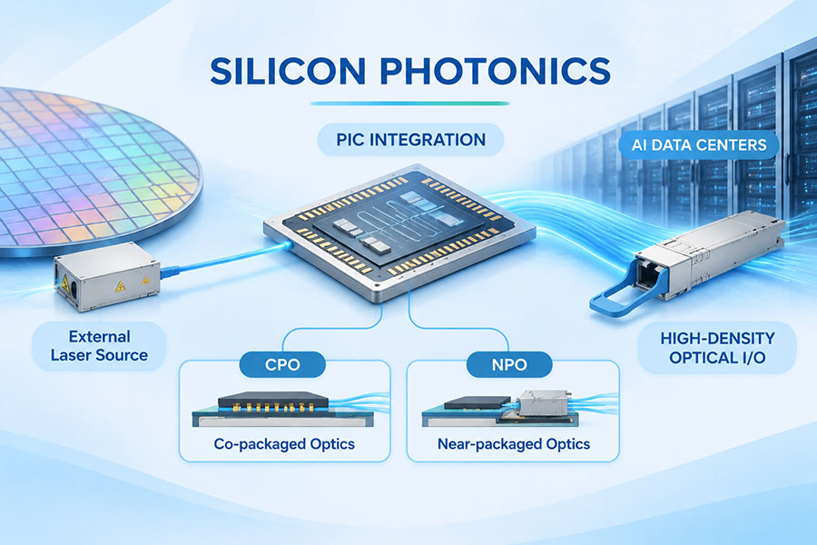
Integrated photonics provides an enabling component technology for several of these architectures. However, PIC integration and package placement are separate design decisions. A photonic chip can be used inside a conventional pluggable transceiver, an NPO engine, or a CPO package.
9. Integrated Photonics and Co-Packaged Optics
Co-Packaged Optics is one of the most visible applications of advanced photonic integration. It brings optical engines closer to high-performance switching silicon, reducing the length of high-speed electrical connections between the ASIC and optical conversion functions.
In a conventional pluggable architecture, electrical signals travel from the switch ASIC across the PCB to the front-panel optical module. In a CPO design, the optical engines are positioned within the same package environment as the switch ASIC or closely integrated package structure.
This can provide several potential advantages:
Shorter high-speed electrical paths.
Reduced electrical channel loss in selected architectures.
Greater potential for high-bandwidth integration.
Improved opportunities for system-level power optimization.
Higher optical connectivity density around switching silicon.
However, CPO introduces significant engineering challenges. Optical engines must operate reliably in a demanding thermal environment close to high-power electronic devices. Fiber attachment, laser delivery, package assembly, repairability, and manufacturing yield also require careful consideration.
External laser sources are one approach to separating laser generation from the most thermally demanding package environment. This can provide operational and thermal design flexibility, depending on the architecture.
CPO should therefore be viewed as a system-level integration approach enabled by photonic technologies, rather than as another name for silicon photonics.
10. Power Efficiency and Thermal Management
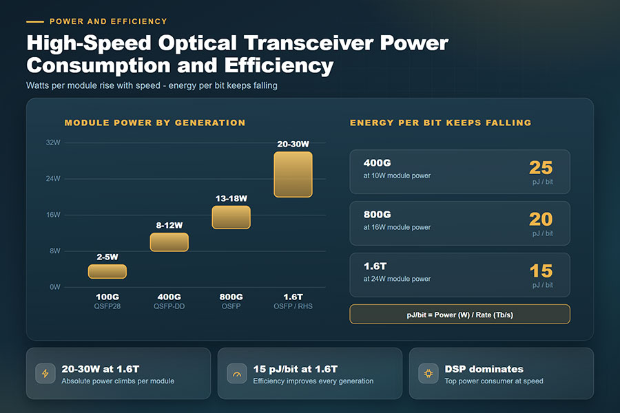
Power consumption is a major consideration in high-speed optical communication. As the number of optical channels and network ports increases, the energy required for signal processing, optical conversion, and thermal management can become substantial.
Integrated photonics may reduce certain optical losses and packaging overheads by combining functions within compact structures. However, integration does not guarantee lower total system power in every implementation.
System power depends on several factors:
Laser efficiency: The optical output required from the light source affects electrical power consumption.
Modulator performance: Drive voltage, capacitance, and bandwidth influence transmitter energy requirements.
Receiver architecture: Photodetector and amplifier performance affect receiver power and sensitivity.
DSP complexity: High-speed signal processing can contribute significantly to module power.
Optical coupling loss: Excessive coupling loss can require additional optical power or reduce system margin.
Thermal design: Package materials, heatsinks, airflow, and cooling arrangements influence operating temperature.
Thermal management becomes especially important in CPO and other densely integrated architectures. Photonic devices may be sensitive to temperature changes, while nearby switch ASICs can generate substantial heat.
Designers must consider thermal isolation, temperature stabilization, wavelength drift, laser operating conditions, and the impact of package materials on long-term reliability.
11. Manufacturing and Packaging Challenges
Integrated photonics has strong potential for high-volume optical communication, but manufacturing and packaging remain important barriers to widespread deployment.
Photonic circuits require precise control of optical dimensions and material properties. Small variations in waveguide geometry, coupling structures, or resonator characteristics can influence optical performance.
Packaging adds another layer of complexity because optical signals must be coupled efficiently between the PIC and external fiber or other optical components.
| Manufacturing Challenge | Technical Impact | Engineering Focus |
|---|---|---|
| Waveguide Fabrication | Dimensional variation can affect optical propagation and loss | Process control and wafer-level inspection |
| Optical Coupling | Misalignment increases insertion loss | Precision alignment and coupling design |
| Laser Integration | Material and thermal differences complicate integration | Hybrid or heterogeneous integration methods |
| Thermal Management | Temperature changes can affect optical performance | Package design and thermal characterization |
| Manufacturing Yield | Defects in individual devices can affect complete PICs | Process optimization and testing strategy |
| Fiber Attachment | High channel counts increase assembly complexity | Automated alignment and reliable optical interfaces |
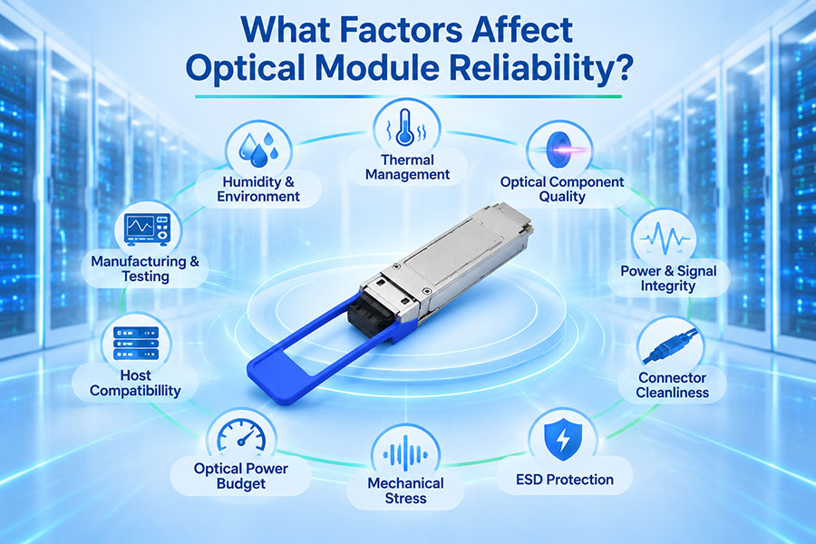
| Reliability | Environmental and mechanical stress can affect long-term operation | Qualification and lifecycle testing |
Testing must cover both individual photonic devices and the completed optical system. Wafer-level optical testing can help identify defective circuits before packaging, while final module testing verifies optical performance, electrical behavior, and environmental stability.
As integration density increases, the cost of testing and repairing a complex photonic package becomes an important part of manufacturing economics.
12. Testing Requirements for Integrated Optical Interconnects
High-speed integrated optical systems require coordinated electrical, optical, and thermal validation. Testing only the photonic chip is insufficient because the final performance depends on the interaction between the PIC, electronic ICs, package, fiber interface, and host platform.
| Test Category | Typical Parameters | Purpose |
|---|---|---|
| Optical Performance | Insertion loss, optical output power, wavelength, and receiver sensitivity | Evaluates optical transmission characteristics |
| Modulator Performance | Bandwidth, extinction ratio, drive requirements, and linearity | Verifies transmitter behavior |
| Photodetector Performance | Responsivity, bandwidth, dark current, and noise | Evaluates optical-to-electrical conversion |
| Electrical Interface | Signal integrity, lane rate, and electrical compliance | Confirms host and electronic integration |
| BER and FEC | Pre-FEC and post-FEC error performance where applicable | Measures link reliability |
| Thermal Performance | Operating temperature, power consumption, and temperature stability | Confirms operation under specified conditions |
| Reliability | Environmental stress and operating-life qualification | Evaluates long-term product stability |
For complete optical modules, interoperability testing is also necessary. The module must operate correctly with the intended switch, NIC, host electrical interface, management software, and fiber infrastructure.
Testing should follow the applicable product specification and interface standards. A photonic device that performs well in isolation does not automatically guarantee a compliant or interoperable optical module.
13. Integrated Photonics in AI Data Centers and Future Computing Systems
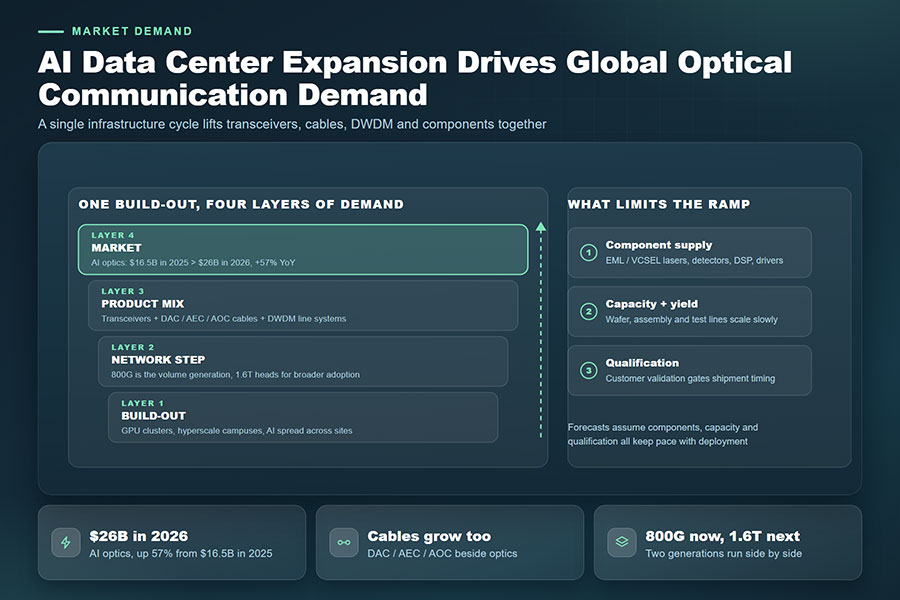
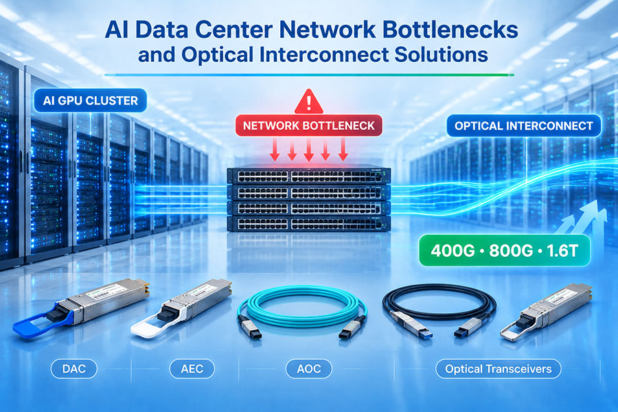
AI data centers are becoming an important application environment for integrated photonics. Large accelerator clusters require high-bandwidth connections between GPUs, switches, memory systems, and storage infrastructure.
As these systems scale, the communication network must provide increasing bandwidth without allowing interconnect power and physical complexity to grow uncontrollably.
Integrated photonics can support several parts of this architecture:
Switch-to-switch connectivity: High-speed optical interfaces provide bandwidth between network switching systems.
GPU cluster networking: Optical transceivers connect distributed computing resources across racks and network tiers.
Optical I/O: Photonic interfaces can support communication between processors and other computing components.
Advanced switching packages: CPO and NPO designs bring optical engines closer to high-bandwidth switch silicon.
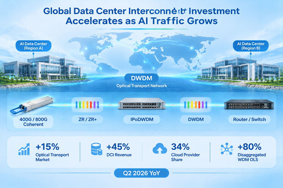
Distributed computing: Optical interconnects support data movement between separate computing systems and facilities.
It is important to distinguish between intra-package optical links, rack-scale optical connections, and data center interconnects. These applications have different requirements for distance, power, latency, serviceability, and optical reach.
Integrated photonics may eventually support a wider range of computing connections, but near-term deployments will continue to use a mixture of pluggable transceivers, optical engines, and conventional electrical links.
14. C-LIGHT High-Speed Optical Connectivity Solutions
Integrated photonics is influencing the development of next-generation optical engines and transceivers. At the system level, high-speed optical connectivity still depends on reliable modules, electrical interfaces, fiber connections, and host compatibility.
C-LIGHT provides optical transceiver solutions for high-speed data center networks, AI infrastructure, and advanced optical communication applications.
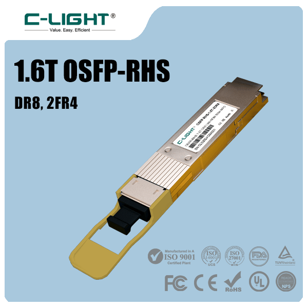
C-LIGHT 1.6T OSFP-RHS Optical Transceiver – Supports 1.6 Tb/s aggregate bandwidth using an 8 × 200G PAM4 architecture with integrated DSP and FEC. Listed configurations include 2DR4 up to 500 m and 2×FR4 up to 2 km over single-mode fiber.
C-LIGHT 800G OSFP Optical Transceiver – Provides multiple configurations for high-speed data center connectivity, including VR8, SR8, DR8, and 2×FR4 variants.
C-LIGHT 800G QSFP-DD Optical Transceiver – Supports high-capacity optical interfaces for compatible data center switching and networking platforms.
C-LIGHT 400G QSFP-DD Optical Transceiver – Offers different optical configurations for data center and high-speed network applications.
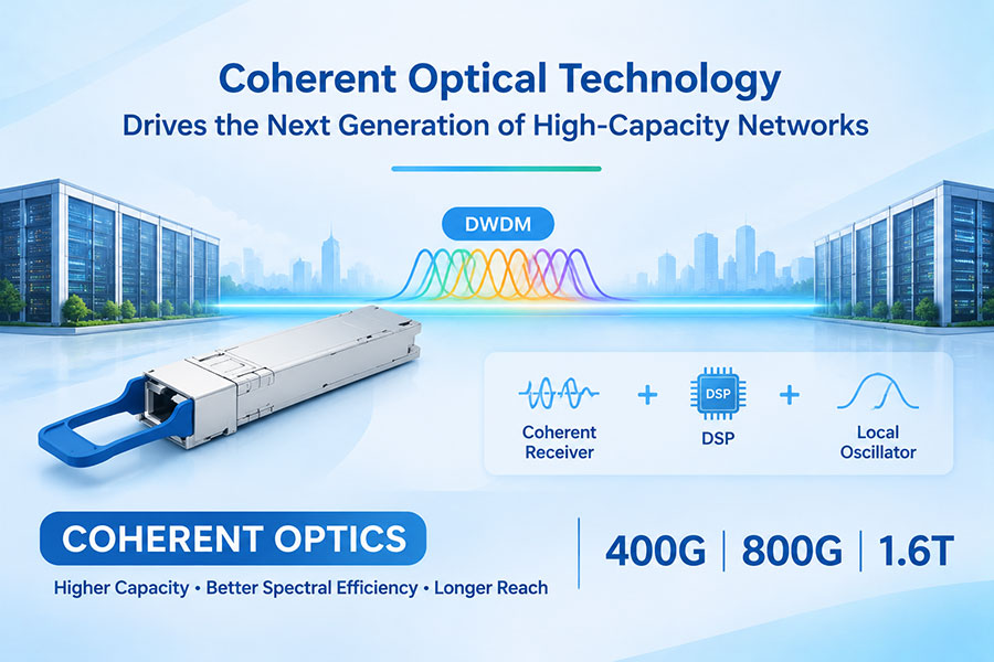
C-LIGHT DWDM DCO Coherent Transceiver – Provides coherent optical connectivity options for high-capacity DCI and DWDM transport applications.
C-LIGHT Optical Transceiver Portfolio – Covers optical connectivity solutions across multiple data rates and application categories.
These products represent pluggable optical connectivity solutions and should not be described as CPO engines or integrated photonic chips unless their individual specifications explicitly identify those technologies. Integrated photonics is a broader technology direction that influences the development of optical components and future transceiver architectures.
For system designers and network operators, selecting a suitable optical solution requires evaluating transmission distance, fiber type, connector configuration, electrical interface, power consumption, thermal requirements, and host compatibility.
15. The Future Development of Integrated Photonics
Integrated photonics is expected to play an increasingly important role as computing and networking systems demand higher bandwidth density and improved energy efficiency. The industry is moving toward more sophisticated combinations of photonic devices, electronic ICs, advanced substrates, and optical packaging.
Several technology directions will shape future development:
Higher-density PICs: More optical functions will be integrated into compact photonic circuits.
Improved heterogeneous integration: Different material platforms will be combined to optimize lasers, modulators, detectors, and waveguides.
Advanced optical packaging: More precise fiber attachment and chip-to-chip optical coupling will support higher channel counts.
CPO and NPO development: Optical engines will move closer to switching silicon in selected high-bandwidth systems.
Optical I/O: Optical links may increasingly connect computing components where electrical interconnects face bandwidth and power constraints.
Manufacturing automation: Improved wafer testing, assembly, and alignment processes will help address production yield and cost.
Standardization: Common interfaces and qualification methods will support broader interoperability.
Research into 2D, 2.5D, and 3D photonic integration is also exploring ways to combine optical and electronic functions at higher levels of density. These approaches remain subject to practical challenges involving heat, manufacturing complexity, reliability, and production scalability.
The development path will not eliminate conventional pluggable optics in the near term. Different architectures will continue to coexist according to their performance, cost, maintenance, and deployment requirements.
16. Conclusion
Integrated photonics is accelerating the evolution of high-speed optical interconnects by combining optical functions into compact and increasingly sophisticated photonic systems. Silicon photonics, photonic integrated circuits, heterogeneous integration, and advanced packaging are helping the industry address the bandwidth and power challenges of next-generation computing networks.
As 800G and 1.6T optical connectivity expands, photonic integration will become increasingly important for improving optical channel density, supporting advanced optical engines, and enabling new packaging architectures such as NPO and CPO.
However, achieving commercial scalability requires more than integrating optical components onto a chip. Manufacturing yield, optical coupling, thermal management, testing, reliability, and interoperability must all be addressed at the system level.
With the continued growth of AI infrastructure, cloud computing, and high-performance networking, integrated photonics is positioned to become an important foundation for future optical communication systems. The combination of advanced photonic devices, electronic integration, and high-speed optical transceivers will shape the next generation of data center connectivity.
For high-speed optical transceivers and data center connectivity solutions, Contact C-LIGHT for product information, technical support, and customized optical networking requirements.
 >

 >
 >
 >
 >
 >
 >
 >