TEL:+86 132 6656 7067





The rapid expansion of artificial intelligence infrastructure is changing the economics and architecture of optical communication. As data center operators increase network bandwidth and connect larger numbers of high-performance computing systems, conventional electrical interconnects face growing challenges in power consumption, signal integrity, and transmission density. Silicon photonics is gaining momentum as an important technology for integrating optical functions with semiconductor manufacturing, supporting the development of higher-capacity and more energy-efficient optical interconnects.
Industry progress is no longer limited to laboratory demonstrations and research projects. Developments in silicon photonic integrated circuits, 12-inch wafer manufacturing, optical packaging, and co-packaged optics are moving the technology closer to broader commercial deployment. These changes are creating opportunities across the optical communication supply chain, from photonic chip design and laser sources to optical engines, transceivers, and high-density fiber connectivity.
1. AI Data Center Expansion Accelerates Silicon Photonics Demand
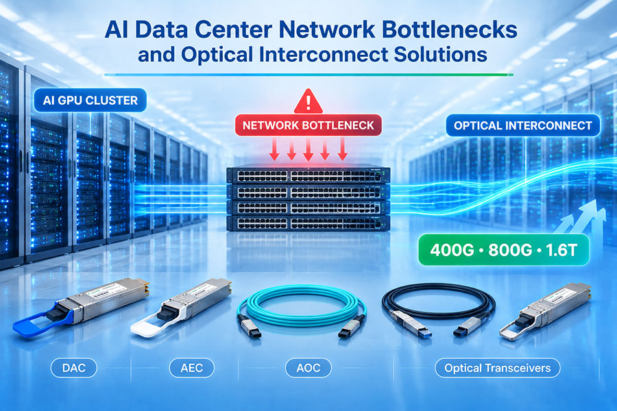
AI training and inference workloads require increasingly large volumes of data to move between processors, memory systems, switches, and storage infrastructure. As AI clusters expand, the network connecting these components becomes a major factor in overall system performance and energy efficiency.
Traditional copper interconnects remain useful for short-distance connections, particularly where cost and simplicity are important. However, increasing data rates and longer electrical paths create challenges involving insertion loss, equalization, signal integrity, and power consumption. Optical communication provides an alternative for connections where bandwidth density and transmission distance become more demanding.
Silicon photonics supports this transition by integrating optical waveguides, modulators, photodetectors, and other photonic functions onto semiconductor-based platforms. Its compatibility with established semiconductor manufacturing techniques provides a potential path toward higher-volume production and more compact optical integration.
Several industry trends are strengthening demand:
Higher network bandwidth: AI clusters require faster connections between computing nodes and network switches.
Increasing rack density: More computing capacity within each rack places additional pressure on interconnect bandwidth and power efficiency.
Scale-up network development: High-performance systems need increasingly dense connections between accelerators and other computing resources.
Energy efficiency requirements: Reducing the power consumed by data movement is becoming an important infrastructure objective.
Manufacturing scalability: Semiconductor-based photonic integration offers opportunities to improve production consistency and support larger deployment volumes.
These requirements are helping silicon photonics move from a specialized optical technology toward a more important part of next-generation data center infrastructure.
2. Silicon Photonics Moves Toward High-Volume Manufacturing
Manufacturing scalability is one of the most important factors determining the commercial development of silicon photonics. A technology may demonstrate strong optical performance in a research environment, but commercial adoption also depends on production yield, packaging consistency, reliability, cost, and the ability to manufacture large quantities of devices.
A notable industry milestone occurred on July 14, 2026, when UMC and SILITH Technology announced the first mass-production wafer delivery of photonic integrated circuits from UMC's Singapore 12-inch fabrication facility. The announcement described a manufacturing platform intended to support high-speed optical interconnects for AI and hyperscale data center networks.
The companies also outlined a roadmap extending from existing 200G-per-lane silicon photonics development toward 400G-per-lane optical interconnect technology. The announcement indicates that the industry is working to connect photonic chip development with established semiconductor manufacturing capabilities.
This development is significant because larger wafer manufacturing platforms can help support production scaling, process integration, and more predictable manufacturing capacity. However, wafer delivery is only one stage of the commercial process. Optical packaging, laser integration, device testing, thermal management, and system-level qualification remain essential before products can be deployed at scale.
3. CPO and NPO Create New Opportunities for Silicon Photonics
Silicon photonics is closely connected to the development of more integrated optical interconnect architectures. Co-packaged optics (CPO) and near-packaged optics (NPO) are receiving increasing attention because they aim to bring optical connectivity closer to switching and computing components.
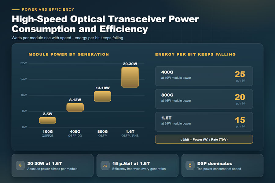
In conventional pluggable optical architectures, transceivers are installed in front-panel ports and connected to switch ASICs through electrical interfaces and circuit-board traces. This approach offers flexibility, serviceability, and a well-established deployment model. As interface speeds increase, however, the electrical path between the switch chip and optical module can become a more significant source of signal loss and power consumption.
CPO places optical engines much closer to the switching or computing ASIC, reducing the length of high-speed electrical connections. NPO also moves optical components closer to the host processor or switch chip, while maintaining a different physical and packaging arrangement from fully co-packaged designs.
| Architecture | Integration Position | Main Characteristics | Potential Applications |
|---|---|---|---|
| Pluggable Optics | Front-panel ports | Replaceable modules, established interfaces, flexible maintenance | Data center switch connections and conventional optical networking |
| NPO | Near the host ASIC | Shorter electrical connections while retaining a separate optical module structure | High-bandwidth AI and data center interconnects |
| CPO | Integrated within or alongside the ASIC package | High optical integration density and reduced electrical interconnect distance | High-radix switches and advanced AI network architectures |
| Optical I/O | Close to computing and processing components | Optical connectivity integrated into broader computing architectures | Future high-bandwidth chip-to-chip and system interconnects |
Silicon photonics is an important enabling technology for these architectures because it can provide compact optical waveguides, modulators, and photonic integration. Nevertheless, the complete optical system also depends on external laser sources, fiber coupling, electronic drivers, thermal design, and advanced packaging.
In May 2026, GlobalFoundries announced its SCALE optical module solution for CPO applications. The platform uses silicon photonics and wavelength-division multiplexing technologies to support bidirectional optical transmission and high-density AI interconnects. This is an example of how silicon photonics is being developed as part of a broader optical packaging ecosystem.
4. Industry Investment Expands Across the Silicon Photonics Supply Chain
The growing demand for optical interconnects is influencing investment across multiple stages of the supply chain. Silicon photonics does not depend on photonic chip manufacturing alone. Commercial products require coordinated development across semiconductor fabrication, laser sources, optical components, packaging, testing, and fiber connectivity.
Several areas are attracting increasing industry attention:
Photonic integrated circuits: Silicon-based platforms integrate optical waveguides, modulators, and photodetectors to support high-speed data transmission.
External laser sources: Many silicon photonics architectures require external light sources, creating demand for reliable and high-power laser solutions.
Advanced optical packaging: Fiber alignment, optical coupling, thermal control, and assembly precision are essential to product performance.
Semiconductor manufacturing: Foundries are developing process platforms and production capacity for photonic integrated circuits.
Testing and qualification: Higher integration density increases the importance of optical, electrical, thermal, and reliability testing.
Manufacturing investment is also being influenced by the need to secure critical materials and components. Indium phosphide (InP) laser technology remains important in many silicon photonics systems because silicon itself is not an efficient light source. This creates a complementary relationship between silicon photonics platforms and other semiconductor materials used for laser generation.
In August 2026, EE Times reported that rising optical networking demand was supporting investment in silicon photonics and advanced packaging. The report also highlighted growing communications and data center business activity, reflecting the broader commercial momentum behind optical infrastructure.
5. Market Forecasts Point to Strong Growth in Integrated Optical Technologies
Market forecasts indicate that silicon photonics and advanced optical packaging could become increasingly important as AI infrastructure expands. These estimates vary depending on how analysts define the market, including whether they measure silicon photonic components, complete optical modules, photonic integrated circuits, or broader optical interconnect systems.
TrendForce published an industry outlook on June 15, 2026, forecasting that the combined CPO and NPO market could exceed US$39 billion by 2030, compared with approximately US$100 million in 2025. The forecast reflects expectations for growing optical integration in AI infrastructure, particularly as data center architectures evolve toward higher bandwidth and more energy-efficient interconnects.
The same report also noted that conventional pluggable optical transceivers are expected to remain a substantial market, with an estimated market value of nearly US$26 billion in 2030. This suggests that integrated optical architectures are likely to develop alongside, rather than immediately replace, established pluggable solutions.
| Market Area | Industry Direction | Key Demand Factors |
|---|---|---|
| Silicon Photonics | Expansion of photonic integration and semiconductor manufacturing | AI networking, hyperscale data centers, high-speed optical modules |
| CPO | Development of optical engines integrated close to switching ASICs | Bandwidth density, power efficiency, high-radix switching |
| NPO | Increasing attention as an intermediate integration architecture | Shorter electrical paths and flexible optical integration |
| Pluggable Transceivers | Continued deployment across data center and telecom networks | Serviceability, interoperability, deployment flexibility |
| Optical Packaging | Greater focus on assembly, fiber coupling, and thermal performance | Higher integration density and manufacturing scalability |
These figures represent forecasts rather than confirmed future revenue. Actual market development will depend on product qualification, manufacturing capacity, system-level reliability, deployment economics, and the pace at which data center operators adopt new architectures.
6. Technical and Manufacturing Challenges Remain
Despite strong industry momentum, silicon photonics still faces technical and manufacturing challenges. Integrating optical and electronic functions into compact packages requires precise control over materials, device structures, optical coupling, and thermal conditions.
Several issues will influence the speed of commercial adoption:
Laser integration: Silicon photonic platforms generally need a separate light source or a hybrid integration approach. Laser performance, coupling efficiency, and reliability are important design considerations.
Optical packaging precision: Fiber-to-chip alignment and optical coupling require accurate assembly processes, particularly as channel counts increase.
Thermal management: High-density optical engines operate alongside power-intensive electronic components, making temperature control important for stability and reliability.
Manufacturing yield: Photonic devices require consistent performance across wafers, dies, and packaged products.
Testing complexity: Integrated devices need coordinated optical and electrical testing, including modulation performance, receiver sensitivity, power consumption, and environmental reliability.
System interoperability: New optical architectures must work with switching platforms, fiber infrastructure, control systems, and network operating requirements.
Packaging and testing are particularly important as the industry moves toward NPO and CPO. A photonic chip with strong component-level performance must still demonstrate reliable operation after integration into a complete optical engine or switch system.
These requirements are encouraging closer collaboration among semiconductor foundries, photonic chip designers, optical component suppliers, packaging specialists, and network equipment manufacturers.
7. Silicon Photonics and the Future of Optical Transceiver Development
Silicon photonics is expected to influence the design of future optical transceivers, but it does not eliminate the need for conventional optical module technologies. Instead, the market is likely to support multiple architectures according to transmission distance, port density, serviceability, power requirements, and system design.
Pluggable transceivers remain important for switch-to-switch and data center interconnect applications. Silicon photonics can be used within certain pluggable module designs, while CPO and NPO target more integrated connections inside high-performance computing and switching systems.
As network speeds advance, the wider optical connectivity ecosystem will continue to require several complementary product categories:
400G and 800G optical transceivers: High-speed modules for data center switching and interconnect applications.
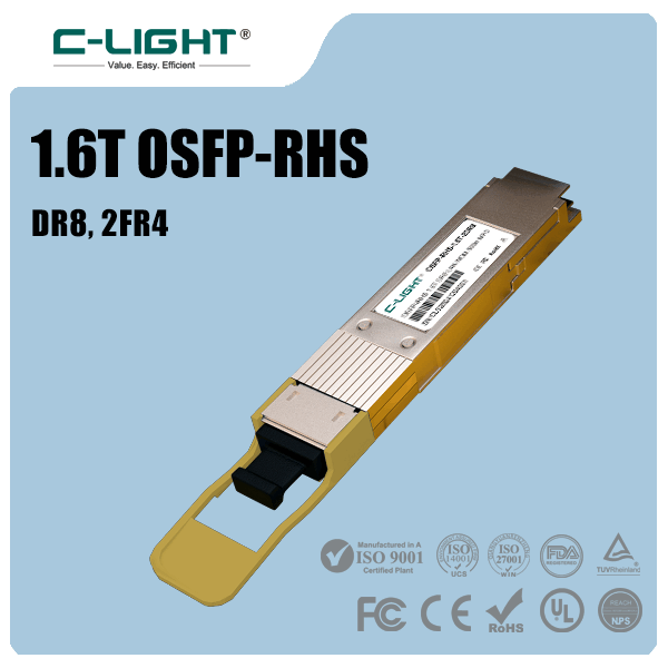
1.6T optical connectivity: Emerging higher-bandwidth solutions for next-generation AI and cloud infrastructure.
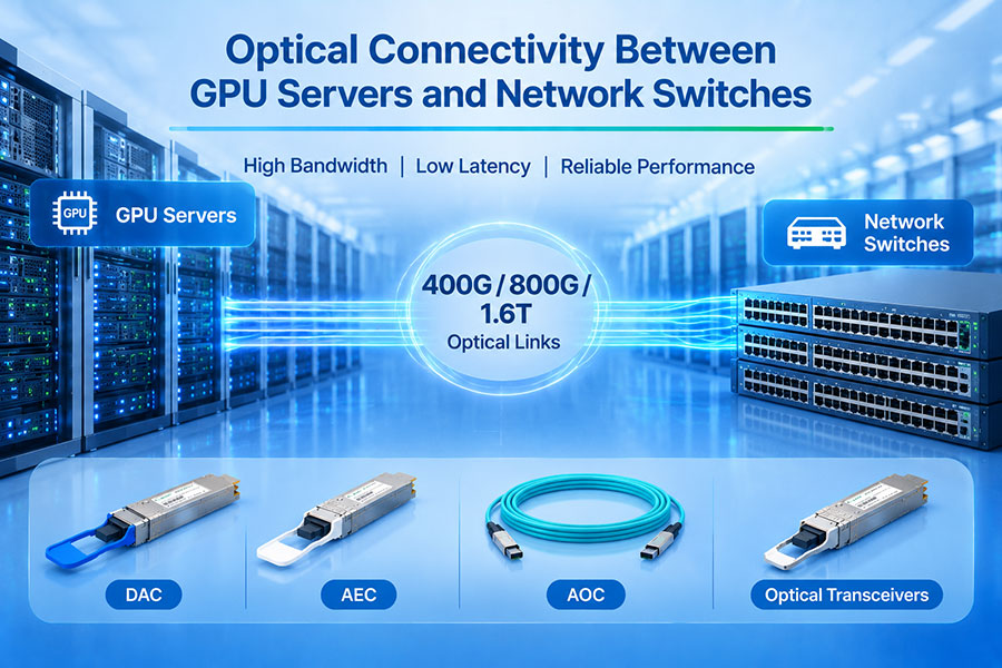
DAC and AEC cables: Electrical interconnect solutions for suitable short-distance connections within racks and between adjacent equipment.
AOC solutions: Active optical cables for high-speed connections where optical transmission and flexible cable routing are required.
DWDM and coherent optics: Technologies supporting higher-capacity optical transport and data center interconnect networks.
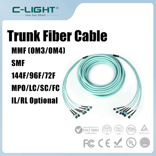
Fiber assemblies and MPO/MTP connectivity: High-density fiber infrastructure supporting optical links across data center environments.
For optical networking projects, C-LIGHT provides a portfolio of optical transceivers and high-speed connectivity products covering data center and telecommunications applications.
8. Industry Outlook: Silicon Photonics Becomes a Strategic Optical Technology
The development of silicon photonics reflects a broader change in the global optical communication industry. Optical connectivity is becoming increasingly important not only for long-distance transmission and data center networking, but also for connections within high-performance computing systems.
AI infrastructure is accelerating this transition by increasing the demand for bandwidth density, lower interconnect power, and scalable network architectures. Progress in 12-inch wafer manufacturing, photonic integrated circuits, external laser sources, and advanced optical packaging is helping the industry move toward more commercially scalable solutions.
However, the transition will not happen through one architecture alone. Pluggable transceivers, NPO, CPO, and future optical I/O technologies are expected to serve different deployment requirements. Their adoption will depend on manufacturing maturity, reliability, system integration, cost, and the practical advantages they provide to network operators.
For the optical communication supply chain, this development creates opportunities across photonic chips, laser sources, optical engines, transceivers, active cables, fiber connectivity, and testing equipment. Companies that can support reliable manufacturing and meet the changing requirements of high-speed networks will play an important role in the next stage of industry development.
As AI data center construction continues and optical integration advances, silicon photonics is positioned to become one of the key technologies shaping the future of global optical communication.
For optical connectivity requirements and product information, please Contact C-LIGHT.
 >

 >
 >
 >
 >
 >
 >
 >