TEL:+86 132 6656 7067





The rapid expansion of AI computing, hyperscale data centers, and high-bandwidth telecommunications networks is changing the requirements of the global photonics manufacturing industry. Optical components that once served primarily as specialized parts of telecommunications equipment are now essential building blocks for large-scale computing infrastructure.
The transition from 400G to 800G and 1.6T optical connectivity is increasing demand for high-performance laser chips, photodetectors, optical engines, photonic integrated circuits, and precision packaging. Manufacturers must improve production capacity while meeting tighter requirements for bandwidth, optical performance, power consumption, and thermal stability.
This shift is also changing the structure of photonics manufacturing. Semiconductor fabrication, optical component production, module assembly, and advanced packaging are becoming more closely connected. Companies with strong capabilities in compound semiconductors, silicon photonics, automated alignment, and high-speed testing are gaining greater importance in the optical communications ecosystem.
1. AI Infrastructure Accelerates Demand for High-Speed Optical Components
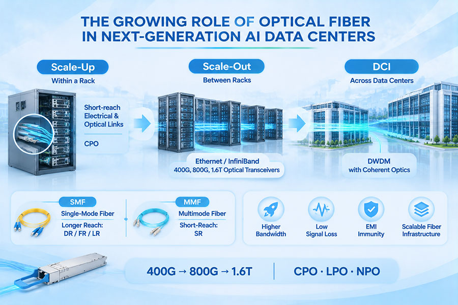
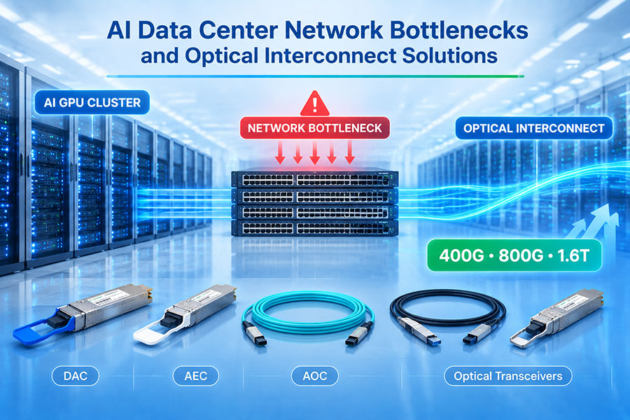
AI data centers require extensive optical connectivity between GPUs, switches, storage systems, and computing racks. As accelerator clusters become larger, the amount of data exchanged between network nodes increases, placing additional pressure on interconnect bandwidth and network capacity.
Optical transceivers support these connections by converting electrical signals into optical signals and recovering data at the receiving end. Higher-speed modules require more advanced optical and electronic components, creating additional manufacturing requirements throughout the photonics industry.
TrendForce projected that the global AI-focused optical transceiver market would grow from approximately US$16.5 billion in 2025 to US$26 billion in 2026. The research identified demand for 800G and faster transceivers, together with constraints in critical optoelectronic components, as major factors influencing industry expansion.
| Market Development | Manufacturing Impact |
|---|---|
| 800G optical deployment | Higher output requirements for lasers, photodetectors, DSPs, and optical subassemblies |
| 1.6T product development | More demanding lane rates, packaging precision, and signal-integrity testing |
| AI cluster expansion | Increased production of optical transceivers, fiber assemblies, and optical engines |
| Power-efficiency requirements | Greater investment in silicon photonics, LPO, NPO, and CPO technologies |
| Higher port density | More compact module designs and advanced thermal-management structures |
The effect extends beyond finished optical modules. Every increase in high-speed transceiver production creates additional demand for upstream semiconductor devices, passive optical components, packaging materials, and manufacturing equipment.
2. InP-Based Laser Manufacturing Becomes a Strategic Industry Segment
Indium phosphide (InP) is a key compound semiconductor material used in high-performance optical communication devices. It supports the production of laser diodes, electro-absorption modulated lasers, and photodetectors used in different optical transmission architectures.
EML technology is particularly important in high-speed optical communication. An electro-absorption modulated laser integrates a laser source and an electro-absorption modulator on a single chip. This structure enables high-speed optical modulation and is used in suitable data center and telecommunications applications.
Manufacturing high-performance EML devices requires specialized epitaxial growth, wafer processing, lithography, device fabrication, and optical characterization. As lane rates increase, maintaining consistent device performance across production batches becomes more challenging.
TrendForce reported in June 2026 that the combined monthly production capacity of EML and CW-DFB laser diodes was expected to reach approximately 50.7 million units during 2026, reflecting substantial capacity expansion by suppliers.
However, additional production capacity does not immediately translate into an equivalent increase in qualified high-performance devices. Manufacturing yield, equipment availability, process optimization, and customer validation all affect the usable output.
Important manufacturing priorities include:
Improving InP wafer quality and epitaxial consistency.
Increasing production efficiency for high-speed EML structures.
Reducing defects during semiconductor processing.
Improving laser output stability and wavelength characteristics.
Expanding high-speed optical characterization capacity.
Maintaining reliability across different operating temperatures.
3. Silicon Photonics Expands the Scope of Photonic Manufacturing
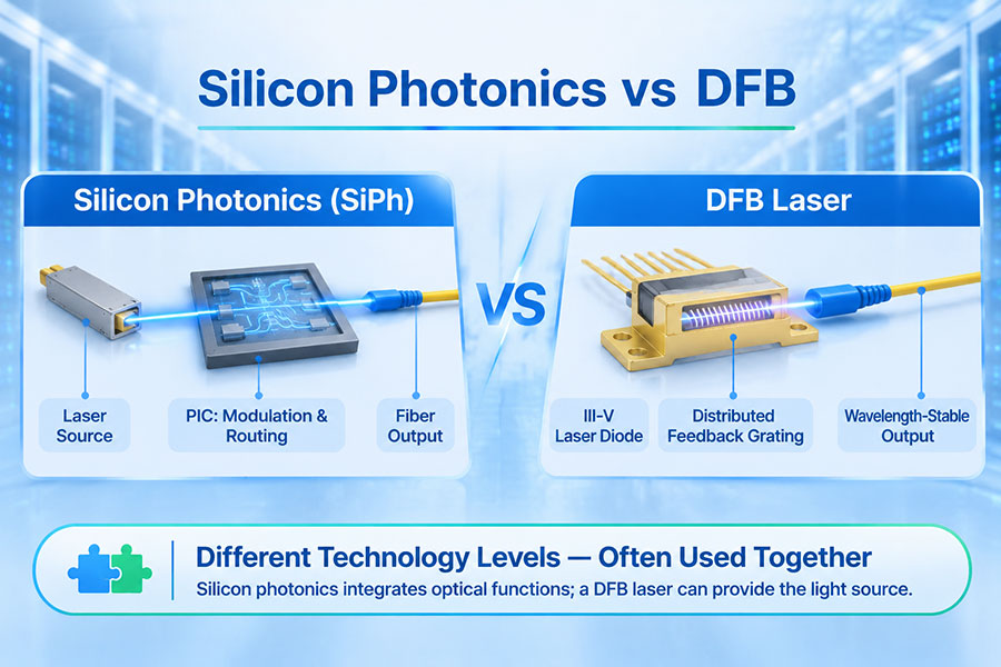
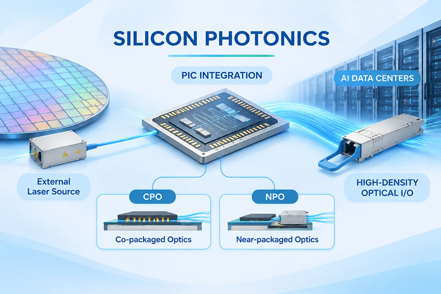
Silicon photonics is becoming an important manufacturing platform for high-bandwidth optical connectivity. It uses silicon-based fabrication processes to create photonic integrated circuits that can perform functions such as optical modulation, splitting, and signal routing.
Compared with traditional discrete optical component architectures, silicon photonics can integrate multiple optical functions into a compact photonic circuit. This creates opportunities for higher integration density and scalable manufacturing.
However, silicon does not efficiently generate light by itself. Silicon photonics systems therefore require suitable external or integrated laser sources, depending on the architecture. Optical coupling, packaging, thermal management, and manufacturing yield remain important challenges.
As AI data center demand grows, manufacturers are investing in several areas:
Silicon photonic wafer fabrication and process optimization.
High-performance continuous-wave laser sources.
Optical coupling between laser sources and photonic integrated circuits.
Low-loss waveguide and modulator structures.
Fiber-array attachment and precision optical packaging.
Wafer-level optical testing and production inspection.
Silicon photonics is not simply replacing conventional optical components. It is creating a different manufacturing ecosystem that combines semiconductor fabrication, laser technology, photonic integration, and advanced packaging.
4. Optical Packaging Becomes More Important as Data Rates Increase
Optical packaging is one of the most technically demanding stages in photonics manufacturing. It connects optical devices, electrical circuits, fibers, lenses, and mechanical structures into a functional assembly.
At higher data rates, small variations in optical alignment, coupling efficiency, electrical interconnection, or thermal behavior can influence module performance. Manufacturers therefore need precise assembly processes and repeatable production controls.
Common optical packaging operations include:
Die attachment and precision component placement.
Active and passive optical alignment.
Laser and photodetector coupling.
Fiber-array attachment and connector integration.
Electrical interconnection and high-speed signal routing.
Thermal interface and heat-dissipation assembly.
Final optical calibration and performance verification.
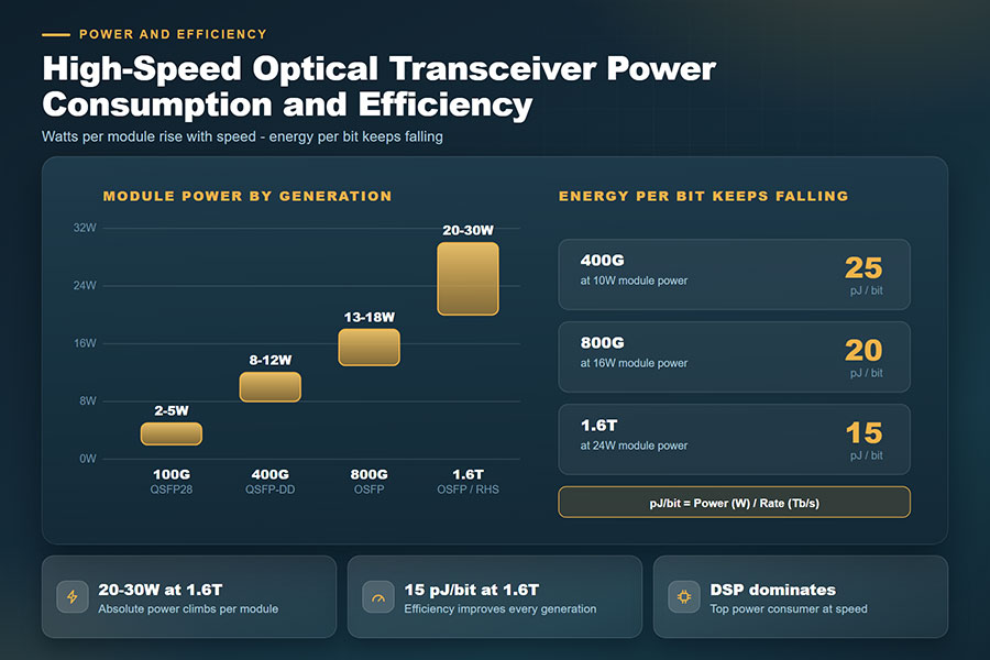
For 800G and 1.6T products, packaging design must accommodate higher bandwidth while maintaining suitable power consumption and operating temperature. The use of multiple optical channels and advanced photonic integration can further increase assembly complexity.
| Packaging Technology | Primary Application | Manufacturing Focus |
|---|---|---|
| Conventional transceiver packaging | Pluggable optical modules | Compact integration, optical alignment, and thermal control |
| Silicon photonics packaging | Integrated photonic circuits | Laser coupling, fiber attachment, and photonic alignment |
| Optical engine packaging | NPO and CPO architectures | High-density optical interfaces and system-level integration |
| High-density fiber-array packaging | Parallel optics and integrated photonics | Precise fiber positioning and low-loss optical coupling |
Packaging capabilities are becoming an important competitive factor because they influence manufacturing throughput, production yield, reliability, and the ability to support new optical architectures.
5. 800G and 1.6T Manufacturing Requires More Advanced Production Equipment
The transition to higher-speed optical modules is increasing the technical requirements of manufacturing equipment. Production lines designed for earlier generations may need upgrades to support higher bandwidth, tighter tolerances, and more complex optical integration.
Manufacturers are investing in automated assembly, precision alignment, high-speed electrical testing, optical measurement, and thermal validation.
Key equipment and process requirements include:
Precision die bonding: Positions optical and electronic components accurately within compact packages.
Active optical alignment: Optimizes coupling between lasers, photonic circuits, lenses, and fibers.
High-speed electrical testing: Validates signal integrity and electrical performance at the target data rate.
Optical characterization: Measures transmit power, wavelength, receiver sensitivity, and other optical parameters.
Thermal testing: Evaluates operating performance under defined temperature conditions.
Automated inspection: Identifies assembly defects and improves production consistency.
Reliability testing: Evaluates product stability under applicable environmental and operating conditions.
Manufacturing throughput is determined by the complete production process. Increasing assembly-line speed alone may not improve total output if optical alignment, calibration, or reliability testing remains a bottleneck.
6. Photodetectors and Optical Receivers Continue to Evolve
Optical communication systems require both transmit and receive components. While laser technology receives significant attention because of its role in high-speed signal generation, photodetectors are equally important for recovering transmitted optical information.
PIN photodiodes and avalanche photodiodes (APDs) are used in different optical receiver designs. Their selection depends on wavelength, sensitivity, bandwidth, noise characteristics, optical power, and application requirements.
As transmission speeds increase, receiver components must maintain sufficient bandwidth and signal quality. Transimpedance amplifiers (TIAs) are also essential because they convert the weak current generated by a photodetector into a usable electrical voltage signal.
Manufacturing priorities for optical receiver components include:
Consistent semiconductor material and device characteristics.
High-speed response and suitable receiver bandwidth.
Low noise and stable sensitivity.
Precise integration with TIA and other electronic components.
Reliable operation across specified temperature ranges.
The receiver side of the optical module therefore requires coordinated development between photodetector manufacturers, analog semiconductor suppliers, and transceiver manufacturers.
7. NPO and CPO Create New Photonics Manufacturing Opportunities
Traditional pluggable transceivers place optical modules at the front panel of network switches. As switch bandwidth increases, the electrical connections between switch ASICs and front-panel modules can create challenges involving power consumption, signal integrity, and thermal management.
Near-packaged optics (NPO) and co-packaged optics (CPO) are emerging architectures intended to bring optical engines closer to high-performance ASICs.
Near-Packaged Optics
NPO positions optical engines near the host ASIC rather than relying exclusively on conventional front-panel pluggable modules. Shorter electrical connections can help address signal-integrity and power challenges in suitable system designs.
This architecture increases demand for compact optical engines, fiber-array units, high-density connectors, and precise optical packaging.
Co-Packaged Optics
CPO integrates optical engines closely with a switch or computing ASIC package. It is intended to reduce the distance that high-speed electrical signals must travel before optical conversion.
CPO introduces additional manufacturing challenges involving photonic integration, laser sources, thermal management, package design, fiber connectivity, and serviceability.
| Technology | Integration Structure | Manufacturing Requirements |
|---|---|---|
| Pluggable optics | Separate optical module installed in a host port | Module assembly, connector integration, and independent testing |
| NPO | Optical engine positioned near the host ASIC | Compact optical packaging, fiber arrays, and thermal design |
| CPO | Optical engines integrated closely with the ASIC package | Advanced co-design, photonic integration, and package-level validation |
These architectures are not immediate replacements for all pluggable transceivers. Their adoption will depend on application requirements, system reliability, manufacturing maturity, operational maintenance, and overall network economics.
8. Global Photonics Manufacturing Capacity Is Expanding
Rising demand for high-speed optical components is encouraging manufacturers to expand production capacity and invest in more advanced manufacturing processes. Capacity expansion is taking place across laser fabrication, photonic integrated circuits, optical packaging, and transceiver assembly.
Different regions contribute different strengths to the global photonics ecosystem. Some have established compound semiconductor and laser manufacturing capabilities, while others specialize in optical component production, precision packaging, electronics integration, or finished transceiver manufacturing.
Manufacturers are evaluating several strategies:
Expanding existing semiconductor fabrication capacity.
Introducing larger wafer platforms where technically and economically suitable.
Automating precision optical assembly and inspection.
Developing additional qualified component sources.
Establishing regional manufacturing and testing capabilities.
Improving production traceability and quality management.
TrendForce reported that suppliers were expanding EML and continuous-wave laser capacity to address AI data center demand. The report also highlighted the importance of high-precision optical manufacturing processes, particularly alignment and packaging, in determining how quickly production can scale.
Despite these investments, new capacity requires equipment installation, process qualification, yield improvement, and customer approval. Announced production capacity should therefore be distinguished from actual qualified output.
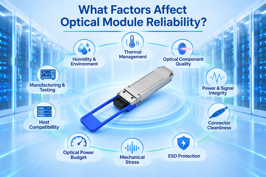
9. Manufacturing Quality and Testing Determine Product Reliability
High-speed optical components must meet defined optical, electrical, mechanical, and environmental requirements. As data rates increase, testing becomes more important because small deviations can affect link performance and product reliability.
For optical transceivers, testing typically covers several categories:
| Test Category | Typical Parameters | Purpose |
|---|---|---|
| Optical transmitter | Output power, wavelength, extinction ratio, optical modulation characteristics | Verifies transmitted optical signal performance |
| Optical receiver | Receiver sensitivity, overload, and relevant error performance | Checks signal recovery capability |
| Electrical performance | Signal integrity, interface performance, and power consumption | Validates host-side electrical operation |
| Thermal performance | Operating temperature and power-related thermal behavior | Checks operation under specified conditions |
| Digital diagnostics | Temperature, voltage, bias current, TX power, and RX power | Supports monitoring and maintenance |
| Reliability | Applicable environmental and endurance tests | Evaluates product stability over time |
Manufacturers also need consistent test procedures and calibrated equipment. Testing results should be traceable to production batches and product configurations to support quality control and customer qualification.
10. C-LIGHT Optical Products for High-Speed Network Applications
The development of AI data centers and high-capacity optical networks is increasing demand for transceivers across multiple data rates and transmission distances. C-LIGHT provides optical connectivity products for data center, telecommunications, and optical transport applications.
400G QSFP-DD Optical Transceivers – Includes SR8, DR4, FR4, LR4, ER4, ZR, and selected coherent configurations for different network distances and applications.
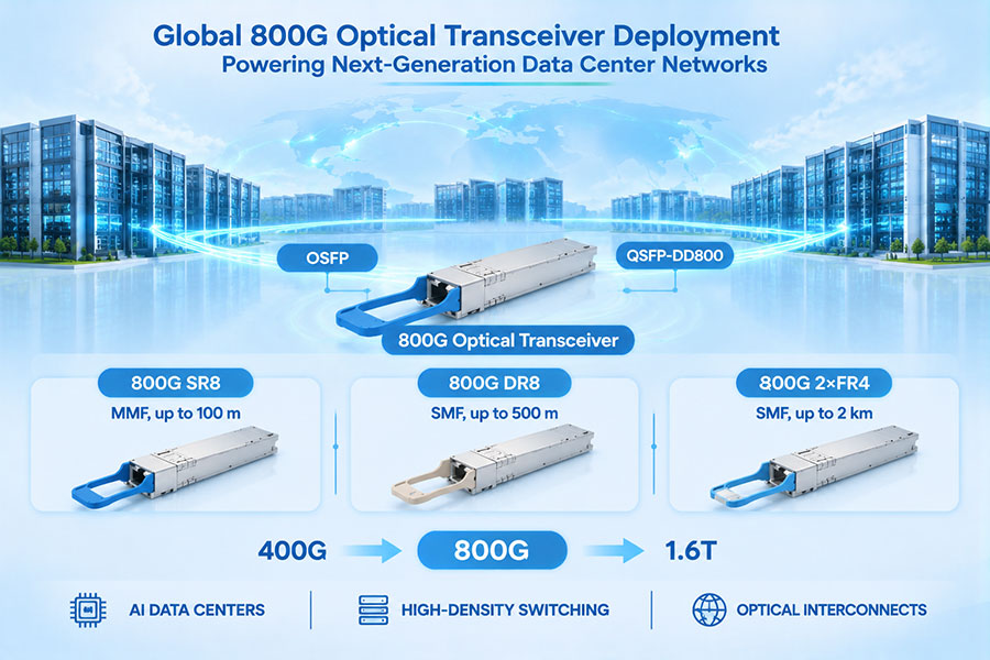
800G OSFP Optical Transceivers – Supports VR8 50m, SR8 100m, DR8 500m, and 2×FR4 2km configurations for high-density data center connectivity.
800G QSFP-DD Optical Transceivers – Provides different optical configurations for high-bandwidth switching and data center interconnection.
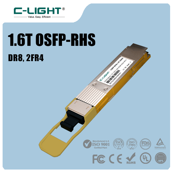
1.6T OSFP-RHS Optical Transceivers – Uses an 8×200G PAM4 architecture with integrated DSP and FEC. Selected configurations support 500m DR4 and 2km 2×FR4 applications.
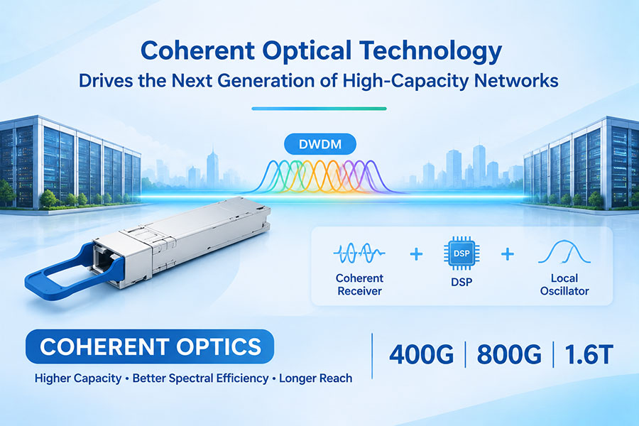
DWDM DCO Coherent Transceivers – Provides coherent optical solutions for high-capacity DWDM transmission and data center interconnection, with reach depending on the specific model and system configuration.
AOC and DAC Connectivity – Active optical and direct-attach cable solutions for suitable short-distance connections in data center and high-performance computing environments.
When selecting optical products, customers should evaluate data rate, reach, wavelength, fiber type, connector interface, host compatibility, power consumption, and thermal requirements. Product specifications and compatibility should be confirmed for the intended network platform before deployment.
11. The Future of Photonics Manufacturing
The global photonics manufacturing industry is entering a period of structural development. AI infrastructure is increasing demand for high-speed optical components, while new integration technologies are changing how optical devices are designed, produced, and tested.
Higher-speed semiconductor devices: EML, continuous-wave lasers, photodetectors, and high-speed electronic components will continue evolving to support 200G-class lanes and future transmission generations.
More integrated photonic platforms: Silicon photonics and other photonic integration technologies will create new manufacturing requirements for wafer fabrication, optical coupling, and advanced packaging.
Advanced packaging capabilities: Precision alignment, fiber-array integration, thermal structures, and package-level testing will become increasingly important.
Automated manufacturing: Greater use of automated inspection, alignment, and testing can improve repeatability and help manufacturers scale production.
Regional capacity development: Manufacturers will continue evaluating production locations and supplier networks to improve delivery flexibility and supply-chain resilience.
Energy-efficient optical architectures: LPO, NPO, and CPO will encourage closer collaboration between photonics manufacturers, semiconductor suppliers, and network equipment developers.
The companies best positioned for this transition will be those capable of combining advanced device technology with reliable high-volume manufacturing, strong quality systems, and close customer engineering collaboration.
12. Conclusion
High-speed optical component demand is reshaping the global photonics manufacturing industry. AI data center expansion and the transition to 800G and 1.6T connectivity are increasing requirements for laser chips, InP materials, photodetectors, silicon photonics, optical engines, and advanced packaging.
Manufacturing competitiveness increasingly depends on more than component design. Semiconductor process capability, optical alignment, assembly yield, testing capacity, thermal performance, and supply-chain coordination all influence the ability to deliver high-performance optical products at scale.
As NPO, CPO, and silicon photonics continue to develop, the photonics manufacturing ecosystem will become more integrated and technically demanding. Reliable production capacity and consistent product quality will remain essential to supporting next-generation AI and telecommunications infrastructure.
For 400G, 800G, 1.6T, and DWDM optical connectivity requirements, Contact C-LIGHT for product information, technical support, and customized optical networking solutions.
 >

 >
 >
 >
 >
 >
 >
 >