TEL:+86 132 6656 7067





AI data centers are placing unprecedented demands on network bandwidth, interconnect density, and power efficiency. Large GPU clusters exchange massive volumes of data across servers and switches, making the electrical connections inside high-performance networking equipment increasingly difficult to scale. Silicon photonics is gaining attention as a way to integrate optical functions more closely with electronic systems and support the next generation of high-speed connectivity.
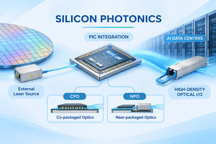
By combining silicon-based photonic circuits with laser sources, photodetectors, and electronic control components, silicon photonics can enable compact optical engines and high-density optical interfaces. The technology is relevant to pluggable transceivers as well as emerging near-packaged optics (NPO) and co-packaged optics (CPO) architectures.
As AI infrastructure moves toward 800G, 1.6T, and higher aggregate bandwidth, silicon photonics is becoming an important part of the industry's strategy for improving interconnect capacity. Its long-term impact will depend not only on photonic integration, but also on packaging, thermal management, manufacturing yield, reliability, and compatibility with network systems.
1. AI Data Center Growth Increases the Need for Optical Interconnects
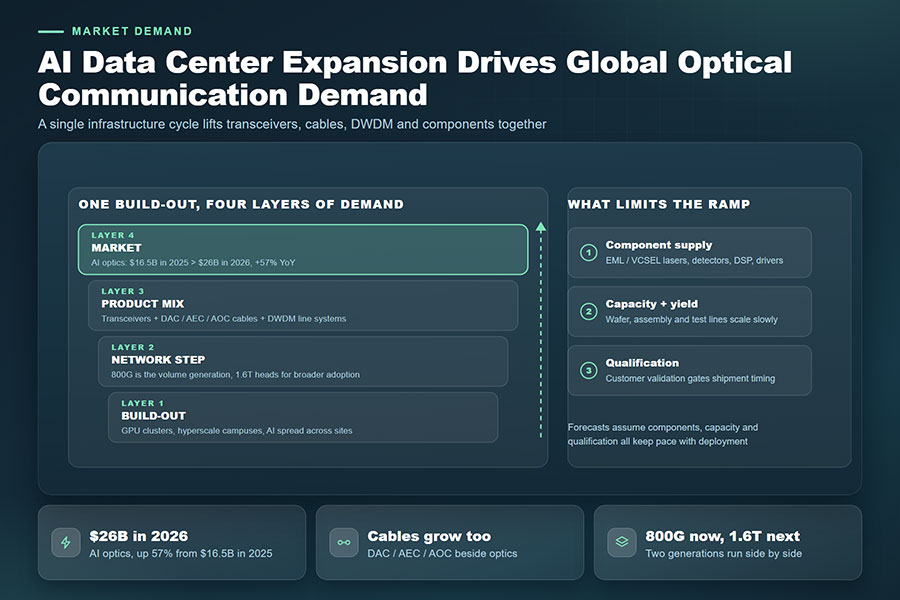
Modern AI infrastructure relies on large clusters of GPUs and other accelerators working together. During model training, computing nodes repeatedly exchange parameters, gradients, and intermediate data. In inference environments, distributed accelerators and storage systems also need high-throughput connections to serve workloads efficiently.
Traditional electrical interconnects remain important within servers and across short distances. However, as signaling rates and connection density increase, electrical channels face challenges involving insertion loss, signal integrity, power consumption, and reach.
Optical interconnects address many of these challenges by carrying data over fiber rather than relying entirely on high-speed electrical transmission across longer board-level or rack-level connections.
Several factors are increasing interest in silicon photonics:
Higher aggregate bandwidth: AI clusters require faster connections between accelerators, switches, and storage systems.
Greater port density: Network equipment needs to support more bandwidth within limited physical space.
Power efficiency: Electrical signal conditioning and long high-speed copper traces can contribute significantly to system power consumption.
Compact integration: Photonic integrated circuits can combine multiple optical functions within a small footprint.
Scalable manufacturing: Silicon-based fabrication offers opportunities to use established semiconductor manufacturing methods for photonic integration.
These requirements are encouraging cloud providers, semiconductor companies, optical component suppliers, and network equipment manufacturers to invest in silicon photonics and related optical integration technologies.
2. What Silicon Photonics Contributes to Optical Connectivity
Silicon photonics is a technology platform that uses silicon-based photonic integrated circuits (PICs) to generate, guide, modulate, split, and detect optical signals, depending on the device architecture and integrated materials.
Instead of assembling every optical function from separate discrete components, silicon photonics can integrate multiple passive and active optical functions onto a photonic chip or combine them through heterogeneous integration.
A typical silicon photonics optical engine may include several functional elements:
| Component | Primary Function | Role in the Optical Engine |
|---|---|---|
| Laser source | Generates optical power | Provides the light required for data transmission |
| Optical modulator | Encodes electrical data onto an optical carrier | Creates high-speed optical signals |
| Waveguide | Guides light through the photonic circuit | Connects integrated optical functions |
| Optical coupler | Transfers light between waveguides, fibers, or other optical devices | Supports optical input and output interfaces |
| Photodetector | Converts received light into an electrical signal | Enables optical signal reception |
| Multiplexer and demultiplexer | Combines or separates wavelength channels | Supports wavelength-division optical architectures |
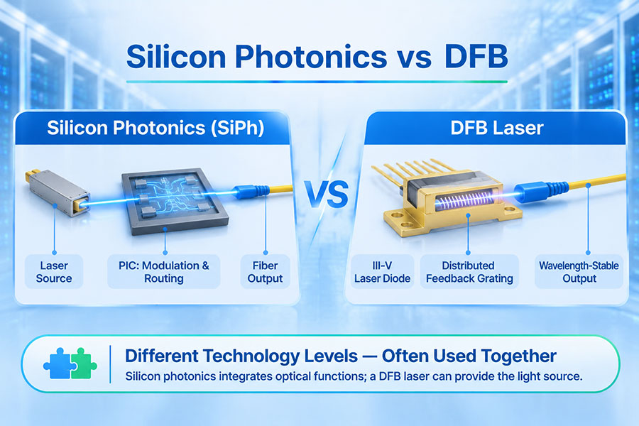
Not every silicon photonics implementation integrates all these functions on one chip. In particular, silicon is not an efficient light source by itself. Many designs use external lasers or integrate suitable III-V semiconductor materials with silicon photonic circuits.
The resulting architecture combines the strengths of different materials and semiconductor technologies to provide optical functionality in a compact package.
3. How Silicon Photonics Supports Higher Bandwidth Density
One of the main attractions of silicon photonics is its ability to integrate multiple optical functions into a relatively compact photonic circuit. This can help reduce the number of discrete optical components and create opportunities for higher-density optical interfaces.
In a conventional optical transceiver, multiple components must be assembled and aligned within a limited module space. A silicon photonics design can integrate waveguides, modulators, splitters, and other optical functions on a PIC, while external components provide the remaining functions.
For AI data centers, higher bandwidth density is important because switch platforms and accelerator systems have limited space for physical connections. As aggregate switch capacity increases, optical integration can help support more data throughput within a constrained footprint.
Silicon photonics can contribute to:
Compact optical engine designs.
Integration of multiple optical channels.
Reduced dependence on some discrete optical assemblies.
High-density fiber connectivity.
Scalable photonic circuit manufacturing.
Optical interfaces for advanced switch and accelerator packages.
However, bandwidth density depends on the complete optical and electrical design. Photonic integration alone does not guarantee lower system power or higher performance. Laser efficiency, driver design, DSP requirements, coupling losses, packaging, and thermal behavior all influence the final result.
4. Silicon Photonics in 800G and 1.6T Optical Transceivers
The transition to 800G and 1.6T optical connectivity is increasing the need for advanced photonic integration. Higher aggregate data rates require faster electrical interfaces, improved optical modulation, and careful management of power and thermal constraints.
Silicon photonics can be used in selected transceiver architectures to integrate optical functions and support multiple high-speed lanes. The exact implementation varies according to data rate, reach, wavelength arrangement, modulation format, and module form factor.
| Data Rate | Network Role | Silicon Photonics Relevance |
|---|---|---|
| 400G | Data center switching and interconnection | Supports integrated optical functions in suitable transceiver designs |
| 800G | AI clusters and hyperscale data centers | Enables compact multi-lane optical engines and higher-density connectivity |
| 1.6T | Next-generation AI networking | Provides a platform for further optical integration and advanced packaging |
| Beyond 1.6T | Future high-bandwidth network architectures | May support more integrated optical engines and chip-level interconnects |
It is important to distinguish data rate from optical technology. Not every 800G or 1.6T transceiver uses silicon photonics. EML-based designs and other optical architectures remain relevant, and the most suitable technology depends on transmission distance, cost, power, performance, and manufacturing considerations.
As the industry moves toward higher lane rates, silicon photonics is expected to play a larger role in selected short-reach and high-density optical connectivity applications.
5. External Laser Sources and Photonic Integration
Laser integration is one of the central engineering considerations in silicon photonics. Silicon waveguides and modulators can perform important optical functions, but a practical system still needs a reliable light source.
One approach is to use an external continuous-wave laser that supplies light to one or more silicon photonic circuits. This separates the light-generation function from the photonic modulation and routing functions.
External laser architectures can provide flexibility in laser selection, replacement, and thermal isolation. They can also simplify certain photonic integration processes because the laser does not need to be fabricated directly on the silicon photonic wafer.
Another approach uses heterogeneous or hybrid integration to combine III-V laser materials with silicon photonic platforms. This can create more integrated optical devices, but introduces additional manufacturing and packaging complexity.
| Laser Architecture | Integration Method | Key Considerations |
|---|---|---|
| External laser | Laser source is separate from the silicon photonic circuit | Optical coupling, fiber routing, laser power, and serviceability |
| Hybrid integration | Laser and silicon photonic components are combined through assembly or bonding | Alignment accuracy, bonding quality, and thermal management |
| Heterogeneous integration | Different semiconductor materials are integrated within a photonic platform | Material compatibility, fabrication processes, and production yield |
Laser architecture affects reliability, optical power delivery, packaging design, and maintenance. For high-volume AI data center deployments, these factors must be evaluated at both component and system levels.
6. Silicon Photonics Enables New NPO and CPO Architectures
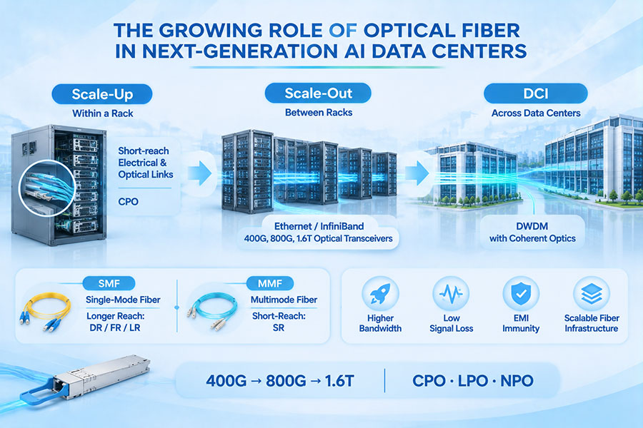
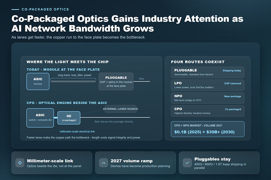
As switch ASIC bandwidth increases, the electrical connections between the ASIC and conventional front-panel optical modules can become a significant design challenge. NPO and CPO are being developed to position optical engines closer to high-performance electronic chips.
Near-Packaged Optics
NPO places optical engines near the host ASIC, generally on or near the same board or package substrate, depending on the implementation. The shorter electrical path can help reduce signal-integrity challenges and the power associated with electrical signal conditioning.
Silicon photonics can provide the integrated optical functions required by NPO engines. The manufacturing ecosystem also needs suitable laser sources, fiber-array units, connectors, packaging materials, and thermal solutions.
Co-Packaged Optics
CPO integrates optical engines closely with a switch or computing ASIC package. The objective is to convert electrical signals into optical signals near the processing chip, reducing the distance traveled by high-speed electrical signals.
TrendForce reported in June 2026 that CPO and NPO market growth is expected to accelerate as AI training and inference systems require greater bandwidth density and improved energy efficiency. Its forecast projected the combined market to grow from approximately US$100 million in 2025 to more than US$39 billion by 2030.
This forecast reflects an emerging market opportunity rather than guaranteed deployment across all data center architectures. Adoption will depend on cost, reliability, manufacturing maturity, maintenance, and system-level benefits.
| Architecture | Optical Engine Position | Potential Benefit |
|---|---|---|
| Pluggable optics | Front panel of the network switch | Replaceable modules and an established deployment model |
| NPO | Near the host ASIC | Shorter electrical paths and closer optical integration |
| CPO | Integrated closely with the ASIC package | High-density optical I/O and reduced electrical interconnect distance |
Silicon photonics is a key enabling platform for many NPO and CPO designs, but these architectures also require advanced electronic packaging, optical coupling, thermal engineering, and system-level validation.
7. Manufacturing and Packaging Challenges Remain Important
Although silicon photonics offers integration advantages, producing reliable optical engines at scale remains technically demanding. Photonic devices must be manufactured with consistent optical characteristics, while packaging must connect the photonic circuit to external lasers, fibers, and electronic components.
Several manufacturing challenges influence product performance and cost:
Optical coupling loss: Light must transfer efficiently between the photonic chip and external fibers or optical components. Poor coupling can reduce link margin and increase system requirements.
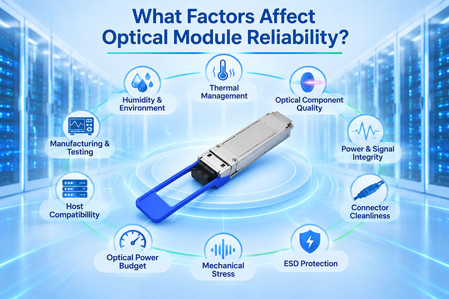
Thermal management: Laser sources, electronic drivers, and nearby ASICs generate heat. Temperature changes can affect laser wavelength, photonic device performance, and long-term reliability.
Packaging precision: Fiber arrays and optical components require accurate alignment. Small positioning errors can affect insertion loss and channel uniformity.
Manufacturing yield: Photonic circuits contain multiple optical structures, and defects in critical devices can reduce the yield of completed optical engines.
Test coverage: Manufacturers need suitable testing at wafer, PIC, optical-engine, and completed-module levels to identify defects at different production stages.
Repair and serviceability: Highly integrated architectures can make component replacement more complex, particularly when optical engines are closely integrated with high-value ASIC packages.
8. Power Efficiency and Thermal Design Influence Adoption
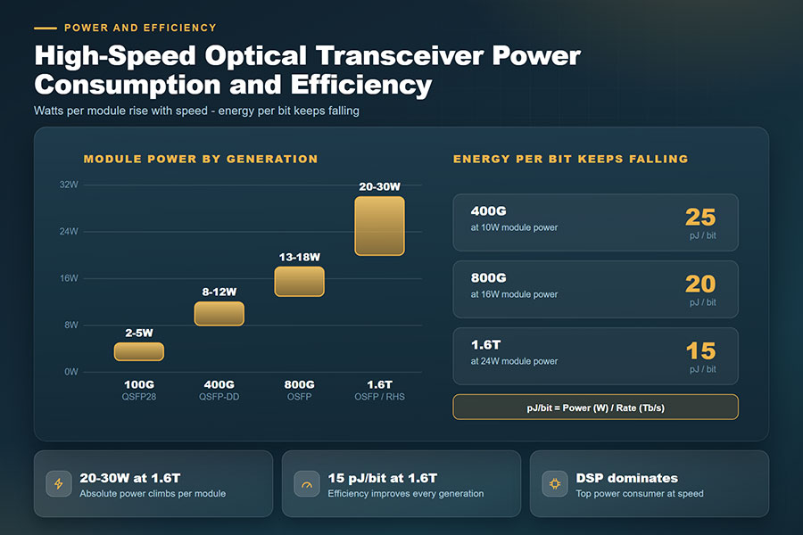
Power consumption is an important consideration in large AI data centers. Thousands of high-speed optical connections can contribute to facility-level electricity demand, making energy per transmitted bit an important design metric.
Silicon photonics can support more integrated optical designs, but it does not automatically consume less power than every conventional optical solution. Actual power depends on the laser architecture, modulator, driver, DSP, optical reach, cooling approach, and system implementation.
NPO and CPO aim to reduce some electrical interconnect losses by bringing optical conversion closer to the ASIC. These approaches may improve system-level energy efficiency in suitable applications, although the optical engine itself still requires power and thermal management.
Important design considerations include:
Laser power and operating efficiency.
Modulator drive voltage and insertion loss.
DSP and electronic signal-conditioning requirements.
Optical coupling efficiency and link margin.
Heat transfer between optical engines and nearby ASICs.
Cooling compatibility and operating temperature limits.
For large-scale deployments, power efficiency should be evaluated across the complete interconnect system rather than from the photonic chip alone.
9. Silicon Photonics and the Future Optical Interconnect Supply Chain
The adoption of silicon photonics is creating a more interconnected supply chain that combines semiconductor manufacturing, photonic device fabrication, laser technology, precision packaging, and optical testing.
Traditional optical transceiver manufacturing often relies on multiple discrete components assembled into a module. Silicon photonics shifts some optical functions into integrated photonic circuits, increasing the importance of wafer fabrication, photonic design, heterogeneous integration, and specialized packaging.
Key participants in the ecosystem include:
Silicon photonics foundries: Fabricate photonic integrated circuits and related devices.
Compound semiconductor suppliers: Provide laser sources and other III-V optical devices.
Electronic semiconductor suppliers: Develop drivers, control ICs, and high-speed signal-processing components.
Optical packaging manufacturers: Integrate PICs, lasers, fibers, and electronic components.
Optical engine developers: Combine photonic and electronic functions into application-specific assemblies.
Network equipment manufacturers: Integrate optical engines into switches, routers, and AI infrastructure.
GlobalFoundries announced its SCALE silicon photonics CPO solution in May 2026, illustrating how semiconductor foundries are developing platforms for optical engines and advanced AI interconnects. Such developments also highlight the need for standard interfaces and coordinated ecosystem development.
As production volumes grow, manufacturing consistency, qualification procedures, component availability, and supply-chain coordination will become increasingly important.
10. C-LIGHT Optical Connectivity for AI Data Center Networks
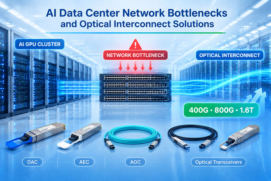
Silicon photonics is one of several technologies supporting the evolution of AI data center connectivity. Network deployments still require optical transceivers and cable solutions selected according to transmission distance, data rate, fiber type, host interface, and system architecture.
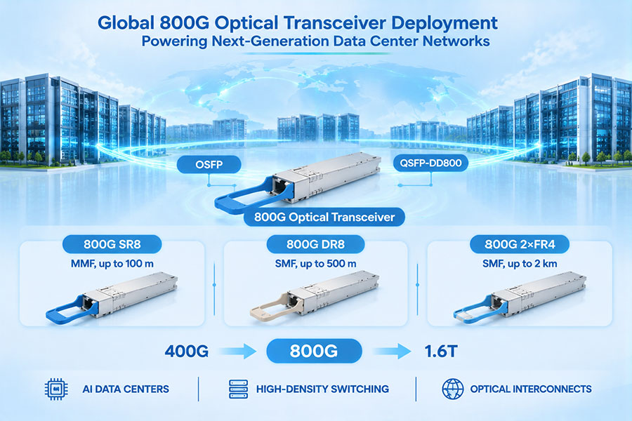
800G OSFP Optical Transceivers – Supports VR8 50m, SR8 100m, DR8 500m, and 2×FR4 2km configurations for AI data centers, cloud networks, and high-performance computing.
800G QSFP-DD Optical Transceivers – Provides high-bandwidth optical connectivity in QSFP-DD form factor for supported data center and networking applications.
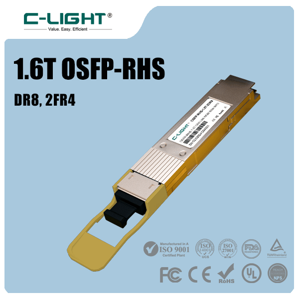
1.6T OSFP-RHS Optical Transceivers – Uses an 8×200G PAM4 architecture with integrated DSP and FEC. Selected configurations support 500m DR4 and 2km 2×FR4 applications.
400G QSFP-DD Optical Transceivers – Offers multiple reach and interface configurations for data center switching and optical interconnection.
AOC and DAC Connectivity – Supports suitable short-distance connections within racks and data centers using active optical or direct-attach cable architectures.
C-LIGHT Optical Transceiver Portfolio – Includes high-speed transceivers, coherent DCO products, and other optical connectivity solutions for different network environments.
These products represent optical connectivity options for AI and data center networks; their inclusion does not imply that every listed module uses a silicon photonics platform. Customers should confirm the optical technology, detailed specifications, and host compatibility of each selected model.
11. Silicon Photonics Will Help Shape Next-Generation AI Networks
The role of silicon photonics is expected to expand as AI infrastructure moves toward higher aggregate bandwidth and more tightly integrated computing systems. Several developments will influence its adoption.
Higher optical lane rates: Continued progress in 200G-per-lane technologies and future higher-speed interfaces will increase the need for advanced photonic devices and electrical-optical co-design.
Greater optical integration: Photonic integrated circuits will combine more optical functions, supporting compact engines and higher-density interconnects.
Wider NPO and CPO development: Advanced packaging will create additional opportunities for silicon photonics in switch and accelerator connectivity.
Improved external laser architectures: Laser integration and distribution will remain important for optical engine reliability, power delivery, and serviceability.
More mature manufacturing ecosystems: Foundries, packaging providers, component suppliers, and network equipment manufacturers will need to improve process compatibility and production standards.
System-level energy optimization: Future optical architectures will be evaluated according to bandwidth density, power consumption, thermal behavior, reliability, and total deployment cost.
Silicon photonics is unlikely to replace every optical technology. Instead, it will coexist with EML-based devices, conventional pluggable modules, coherent optics, and other photonic platforms. The most suitable architecture will depend on the network's reach, bandwidth, cost, and operational requirements.
12. Conclusion
Silicon photonics is becoming an important technology for AI data center connectivity as GPU clusters, high-performance switches, and cloud infrastructure demand higher bandwidth density and more efficient interconnects. By integrating optical functions into silicon-based photonic circuits, the technology creates opportunities for compact optical engines and advanced optical I/O architectures.
Its influence extends from 800G and 1.6T transceivers to NPO and CPO systems. However, successful deployment requires more than photonic integration. Laser sources, optical coupling, packaging precision, thermal management, manufacturing yield, and system reliability all determine the performance of the final solution.
As AI networks continue to scale, silicon photonics will remain an important part of the broader transition toward higher-capacity and more integrated optical connectivity.
For 400G, 800G, 1.6T, and other high-speed optical connectivity requirements, Contact C-LIGHT for product information, technical support, and customized optical networking solutions.
 >

 >
 >
 >
 >
 >
 >
 >