TEL:+86 132 6656 7067





High-speed optical networks depend on signal processing across both electrical and optical transmission paths. Electrical DSP focuses on the conditioning and recovery of electrical signals traveling through SerDes interfaces, PCB traces, connectors, and other electrical channels. Optical DSP is designed for the requirements of optical communication systems, including transmitter waveform preparation, receiver signal recovery, and optical impairment compensation. Although these functions can be integrated into the same semiconductor device, they address different parts of the communication link. Understanding their relationship is essential when designing 400G, 800G, and 1.6T optical connectivity.
1. What Is Electrical DSP?
Electrical DSP refers to digital signal processing applied to electrical communication signals. In high-speed networking equipment, it is commonly associated with SerDes, electrical PHYs, retimers, and other signal-processing circuits that manage data transmission between electronic components.
Electrical signals traveling through PCB traces, package interconnects, connectors, and copper cables experience insertion loss, reflections, crosstalk, jitter, and inter-symbol interference. These effects become increasingly difficult to manage as signaling rates increase.
Electrical DSP uses digital algorithms to improve signal quality and recover transmitted data. Depending on the implementation, it may operate inside a SerDes receiver, a dedicated retimer, or a larger PHY subsystem.
Typical Electrical DSP functions
Transmit equalization: Shapes the electrical output waveform to compensate for channel loss.
Feed-forward equalization (FFE): Applies digital filtering to reduce inter-symbol interference.
Decision-feedback equalization (DFE): Uses previous symbol decisions to compensate for selected post-cursor interference.
Clock and data recovery (CDR): Recovers timing information from incoming serial data.
Adaptive equalization: Adjusts receiver parameters to changing channel conditions.
Signal detection: Determines transmitted symbol values from the received electrical waveform.
Lane alignment: Supports timing alignment and data reconstruction across multiple electrical lanes where implemented.
Electrical DSP is particularly important in high-speed chip-to-chip communication, switch ASIC interfaces, NIC connections, backplanes, and electrical links between host processors and optical modules.
2. What Is Optical DSP?
Optical DSP is digital signal processing designed for optical communication systems. It is commonly integrated into high-speed optical transceivers, coherent optical modules, and optical transmission equipment.
An Optical DSP does not directly manipulate light as a digital processor. Instead, it processes digital representations of electrical signals associated with optical transmission and reception. Optical components perform the actual electro-optical and optoelectronic conversions.
In a direct-detection optical transceiver, the DSP may process the electrical waveform before it reaches the optical driver and after it leaves the receiver's analog front end. In coherent optical systems, it can perform much more extensive processing to recover information encoded in the amplitude and phase of the received optical field.
Typical Optical DSP functions
Transmit waveform processing: Prepares electrical signals for optical modulation.
Digital pre-compensation: Compensates for selected transmitter and channel characteristics.
Receive equalization: Improves the quality of received electrical waveforms.
Clock and timing recovery: Supports symbol synchronization and data recovery.
Optical impairment compensation: Processes dispersion, polarization effects, and phase-related impairments in suitable coherent systems.
Modulation and demodulation: Supports the digital processing required by the selected modulation format.
FEC processing: May implement forward error correction in architectures that integrate FEC into the optical subsystem.
The processing requirements differ significantly between short-reach PAM4 transceivers and long-distance coherent optical modules. Not every Optical DSP performs every function listed above.
3. Optical DSP vs Electrical DSP: Main Differences
| Technical Factor | Electrical DSP | Optical DSP |
|---|---|---|
| Primary Purpose | Processes electrical communication signals | Processes signals associated with optical communication |
| Typical Location | SerDes, electrical PHY, retimer, or host ASIC | Optical transceiver or optical communication subsystem |
| Signal Domain | Electrical channel | Digital processing of electrical representations of optical-link signals |
| Main Channel | PCB traces, connectors, packages, and copper interconnects | Optical transmitter, fiber, receiver, and associated electrical interfaces |
| Equalization | Compensates for electrical channel loss and distortion | May compensate for module and optical-link signal impairments |
| Clock Recovery | Commonly performed in SerDes and retimer receivers | May perform timing recovery and synchronization within the module |
| Optical Dispersion Compensation | Not a standard electrical DSP responsibility | Supported in suitable coherent DSP architectures |
| Polarization Processing | Not a standard electrical DSP responsibility | Important in polarization-multiplexed coherent systems |
| Typical Applications | SerDes links, retimers, electrical PHYs, and high-speed backplanes | 400G/800G optical transceivers, coherent optics, and optical transport |
These are functional distinctions, not mutually exclusive chip categories. An Optical DSP may include electrical SerDes interfaces and electrical equalization functions. Likewise, a host electrical PHY may perform digital processing that directly affects the electrical waveform entering or leaving an optical module.
4. Where Electrical DSP and Optical DSP Work in the Same Link
A conventional DSP-based optical connection can contain several signal-processing stages. The host electrical PHY handles the electrical connection to the module, while the module DSP processes the signal for optical transmission and reception.
Transmit direction
Host ASIC → Electrical DSP / SerDes → High-Speed Electrical Interface
Optical module processingModule Electrical Interface → Optical DSP → DAC / Analog Signal Chain (where applicable) → Driver
Optical conversionLaser or Modulator → Optical Fiber
The host ASIC generates the data and sends it through its electrical PHY. The host SerDes converts the data into high-speed serial electrical lanes and applies the signal conditioning required for the host-to-module electrical channel.
The module DSP then performs the processing required by the optical transmitter architecture. The processed signal reaches the driver, which controls the laser or optical modulator to generate the outgoing optical waveform.
Receive direction
Optical Fiber → Photodetector → TIA
Optical module processingAnalog Front End / ADC → Optical DSP (where implemented)
Host electrical processingElectrical Interface → Host SerDes / Electrical PHY → Host ASIC
The photodetector converts incoming light into electrical current, and the TIA converts that current into a voltage signal. The module's analog front end and Optical DSP process the waveform before it reaches the host electrical interface. The host SerDes then receives the data and reconstructs it for the ASIC.
The exact architecture depends on the transceiver. Some modules use integrated DSP and SerDes functions, while others use separate processing components or linear analog paths.
5. Electrical Equalization vs Optical Signal Compensation
Equalization is used in both electrical and optical communication systems, but the channel impairments being addressed can be different.
Electrical DSP primarily addresses distortions introduced by electrical interconnects. These include frequency-dependent insertion loss, reflections, crosstalk, and inter-symbol interference.
Optical DSP may address electrical distortion within the module as well as impairments associated with the optical transmission system. In coherent systems, the processing can include compensation for chromatic dispersion, polarization-mode dispersion, polarization rotation, and laser phase noise.
| Processing Function | Electrical DSP | Optical DSP |
|---|---|---|
| Electrical Channel Equalization | Core function in high-speed electrical PHYs | May compensate for module-internal electrical paths |
| FFE / DFE | Commonly used in SerDes receivers | May use digital equalization in the optical receiver chain |
| Transmit Pre-Emphasis | Shapes electrical signals for channel transmission | May provide additional optical transmitter pre-compensation |
| CDR | Recovers timing from electrical serial signals | May perform timing and symbol synchronization inside the module |
| Chromatic Dispersion Compensation | Not a normal electrical PHY function | Supported by coherent optical DSP |
| Polarization Demultiplexing | Not a normal electrical PHY function | Used in polarization-multiplexed coherent receivers |
| Phase Recovery | Electrical timing and clock functions may be present | Carrier phase recovery is important in coherent systems |
Electrical equalization and optical impairment compensation should not be treated as interchangeable operations. They address different physical effects, although both can be implemented through digital filtering and adaptive algorithms.
6. Direct-Detection Optical DSP vs Coherent Optical DSP
Optical DSP itself covers different levels of processing complexity. Direct-detection and coherent optical systems have different receiver structures and signal-recovery requirements.
Direct-detection optical systems
In common PAM4 direct-detection transceivers, the receiver uses a photodetector to convert optical intensity into an electrical signal. The TIA amplifies the resulting current, and the receiver processing chain recovers the transmitted symbols.
The Optical DSP may perform equalization, clock recovery, symbol detection, and other signal-conditioning functions. Its purpose is to recover data reliably despite bandwidth limitations, noise, and inter-symbol interference.
Coherent optical systems
Coherent optical systems use a local oscillator laser and coherent detection to recover information encoded in the amplitude and phase of the optical field. The receiver generates electrical I/Q signals, which are digitized and processed by a coherent DSP.
Coherent DSP can perform:
Chromatic dispersion compensation.
Polarization demultiplexing.
Polarization-mode dispersion compensation.
Frequency offset estimation.
Carrier phase recovery.
Adaptive equalization and signal reconstruction.
FEC processing in supported implementations.
These functions are particularly important in coherent 400ZR, ZR+, and other optical transport applications. They are not typical responsibilities of a conventional host SerDes.
7. Power Consumption and Latency
Electrical DSP and Optical DSP contribute to different parts of a system's power budget. Electrical DSP is generally part of the host ASIC, SerDes, retimer, or PHY power consumption. Optical DSP contributes to the optical module or optical subsystem power budget.
High-speed digital equalization, clock recovery, data conversion, and signal-processing operations consume power. At higher lane rates, the processing bandwidth and thermal requirements become more demanding.
The location of the processing also influences latency. A dedicated electrical retimer introduces processing stages in the electrical path. An optical DSP introduces processing stages within the optical module. The total latency depends on the number of stages, implementation, clocking, equalization architecture, and FEC configuration.
| Performance Factor | Electrical DSP | Optical DSP |
|---|---|---|
| Power Location | Host ASIC, electrical PHY, or retimer | Optical module or optical subsystem |
| Processing Workload | Electrical channel conditioning and recovery | Optical-link signal conditioning and recovery |
| Latency Contribution | Depends on electrical PHY and retiming architecture | Depends on optical DSP pipeline and processing functions |
| Thermal Impact | Contributes to host ASIC or retimer thermal load | Contributes to module or optical subsystem thermal load |
| Optimization Focus | Electrical signal integrity and interface efficiency | Optical transmission performance and module efficiency |
There is no universal rule that Optical DSP always consumes more power or has higher latency than Electrical DSP. The two may have very different processing workloads, and their power and latency must be evaluated within the actual implementation.
8. How LPO Changes the Relationship Between the Two
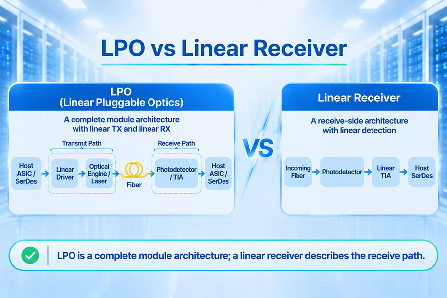
Linear Pluggable Optics (LPO) changes where high-speed signal processing takes place. A conventional DSP-based optical module performs substantial signal conditioning and retiming inside the module. LPO removes conventional in-module DSP retiming from the relevant high-speed paths and relies more heavily on the host SerDes.
In an LPO transmitter, the host electrical PHY generates a waveform that passes through a linear electrical interface and linear driver before reaching the optical transmitter. On the receive side, the photodetector and TIA deliver a linear electrical signal toward the host SerDes.
Host Electrical PHY → Module Optical DSP → Optical Driver → Fiber
Fiber → Photodetector / TIA → Module Optical DSP → Host Electrical PHY
Typical LPO linkHost SerDes → Linear Driver → Optical Transmitter → Fiber
Fiber → Photodetector / TIA → Host SerDes
LPO shifts more of the electrical signal-processing workload to the host. It does not eliminate all digital processing from the system. The host SerDes still performs equalization and timing recovery, and the host PCS or other system blocks may continue to perform FEC and related functions.
This architecture can reduce module power and processing latency, but it requires careful electrical channel design and strong host SerDes capability.
9. Electrical DSP and Optical DSP in 400G, 800G, and 1.6T Networks
The progression from 400G to 800G and 1.6T increases the demands on both electrical and optical signal processing. Higher lane rates require better control of channel loss, timing, noise, and modulation quality.
400G optical connectivity
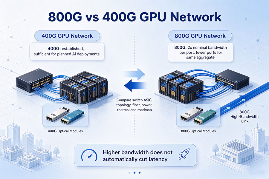
400G systems use different electrical lane configurations depending on the interface. Common examples include four approximately 100G-class lanes or eight approximately 50G-class lanes. Electrical DSP manages the host channel, while Optical DSP supports the module's optical signal-processing requirements where implemented.
800G optical connectivity
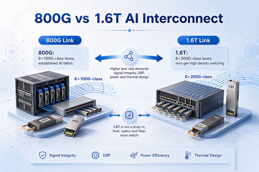
Many 800G optical modules use eight approximately 100G-class electrical lanes. Host SerDes capability, module DSP performance, and optical receiver characteristics must be designed together to maintain the required signal quality and link reliability.
1.6T optical connectivity
Common 1.6T architectures move toward eight approximately 200G-class electrical lanes. The higher signaling rate increases the importance of electrical channel quality and advanced optical signal processing.
The host SerDes must support the required electrical interface, while the Optical DSP must meet the processing demands of the selected optical technology. Neither component alone determines the achievable transmission distance or overall link performance.
| Network Generation | Representative Lane Configuration | Electrical DSP Focus | Optical DSP Focus |
|---|---|---|---|
| 400G | 4 × 100G-class or 8 × 50G-class | Host electrical interface and channel equalization | Module waveform processing and signal recovery |
| 800G | 8 × 100G-class | Higher-rate SerDes and electrical signal integrity | Multi-lane optical signal processing and receiver recovery |
| 1.6T | 8 × 200G-class in common architectures | Next-generation electrical channel and SerDes performance | Higher-bandwidth optical processing and signal compensation |
These are representative architectures rather than universal lane mappings. Actual configurations depend on the applicable Ethernet or optical interface specification and the module design.
10. Compatibility and System-Level Design
Electrical DSP and Optical DSP must be evaluated as parts of a complete communication system. A module's nominal data rate does not fully describe its electrical interface, signal-processing architecture, or optical capabilities.
Before selecting a transceiver or host platform, engineers should verify:
Host SerDes capability: Confirm supported lane rates, signaling formats, and equalization functions.
Electrical channel: Evaluate PCB insertion loss, return loss, crosstalk, and connector performance.
Module architecture: Identify whether the optical module uses a full DSP, partial retiming, or a linear signal path.
Optical interface: Verify wavelength, modulation format, fiber type, connector, and transmission distance.
Receiver performance: Check sensitivity, overload limits, and required BER performance.
FEC allocation: Confirm whether FEC is implemented in the host PCS, optical DSP, or another system component.
Power and cooling: Evaluate the combined power consumption and thermal requirements of the host and optical module.
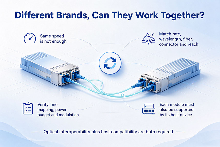
Interoperability: Validate the exact switch, NIC, firmware, and transceiver combination.
A module with an Optical DSP and a module using a linear architecture may share the same OSFP or QSFP-DD form factor. Their electrical behavior and host requirements can still differ. Form factor and data rate alone do not establish interoperability.
11. C-LIGHT Optical Transceiver Solutions
High-speed optical connectivity requires coordinated electrical and optical signal processing. Host SerDes capability, module architecture, optical reach, fiber infrastructure, and power requirements all contribute to the performance of the complete link.
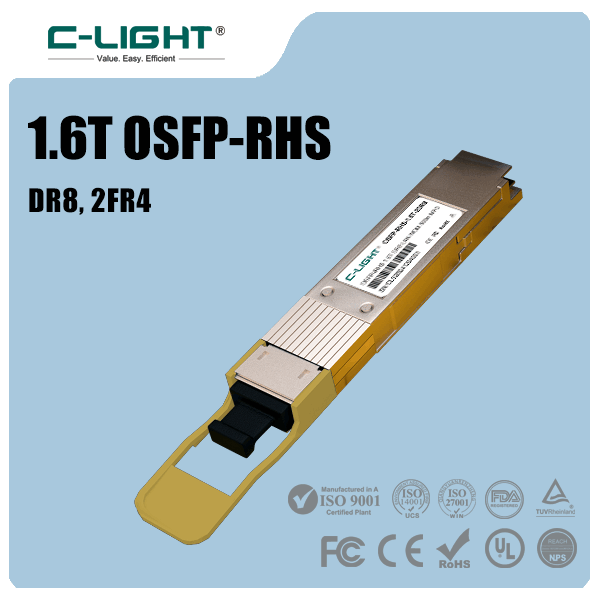
C-LIGHT provides optical transceiver solutions for data center, enterprise, and telecommunications networks. The C-LIGHT Optical Transceiver portfolio provides a starting point for evaluating modules across different speeds and applications.
For 400G, 800G, and 1.6T deployments, selecting the correct transceiver requires more than matching the nominal data rate. The host electrical interface, DSP architecture, optical wavelength, fiber type, connector, transmission distance, and power budget should all be considered.
C-LIGHT's Optical DSP technical guide provides additional background on the signal-processing functions used in high-speed optical modules.
For optical transceiver selection, platform compatibility, and customized connectivity requirements, Contact C-LIGHT.
12. Conclusion
Electrical DSP and Optical DSP perform different but complementary roles in high-speed communication systems. Electrical DSP focuses on electrical channel conditioning, equalization, timing recovery, and data reconstruction. Optical DSP processes signals associated with optical transmission and reception, including transmitter waveform preparation, receiver recovery, and advanced optical impairment compensation.
The distinction is based on processing responsibility rather than a strict separation between two chip categories. An Optical DSP can contain electrical signal-processing functions, and modern SerDes devices already perform sophisticated digital equalization.
In conventional DSP-based optical modules, host electrical processing and module optical processing share the workload. In LPO architectures, more responsibility moves to the host SerDes, reducing module processing overhead while increasing the importance of electrical channel quality.
As optical networks advance toward 800G and 1.6T, understanding how electrical and optical signal processing interact is essential for designing reliable links, selecting compatible transceivers, managing power consumption, and maintaining end-to-end signal integrity.
 >

 >
 >
 >
 >
 >
 >
 >