TEL:+86 132 6656 7067





At 400G, 800G, and 1.6T data rates, the optical transmitter must convert high-speed electrical signals into precisely controlled optical waveforms. The architecture of the transmitter driver determines how the electrical signal is conditioned before reaching the laser or optical modulator. A linear driver maintains a more direct analog signal path, while a DSP-based transmitter uses digital processing to manage signal conditioning and other functions before the final electrical drive stage. This difference affects module power, latency, signal integrity, and the capabilities required from the host ASIC.
1. What Is a Linear Driver?
A linear driver is an analog electronic circuit that amplifies and conditions an electrical signal while maintaining a substantially linear relationship between its input and output over the specified operating range. In an optical transmitter, it drives a laser or external optical modulator according to the electrical waveform received from the host.
Unlike a conventional DSP-based transmitter architecture, a linear-drive implementation does not rely on an in-module DSP to perform the full digital equalization and retiming process in the transmit path. Instead, the host ASIC or NIC SerDes performs much of the signal conditioning before delivering the electrical waveform to the optical module.
The linear driver provides the electrical amplitude and drive capability required by the optical device. Depending on the transmitter design, it may also include analog gain control, pre-emphasis, or other supporting functions. These functions do not make it a DSP.
Typical linear transmitter signal path
Host ASIC / NIC → SerDes → Transmit Equalization
Module-side electrical drive:Linear Electrical Interface → Linear Driver
Optical conversion:Laser or Optical Modulator → Optical Fiber
The main objective is to reduce the amount of digital processing inside the optical module. This can lower module power and processing latency, particularly in short-reach data center applications where the host SerDes and electrical channel can be tightly controlled.
2. What Is a DSP-Based Driver Architecture?
The term DSP driver is commonly used when discussing DSP-based optical transmitter architectures, but it is important to distinguish the DSP from the physical modulator driver. The DSP performs digital signal processing, while the driver is an analog circuit that supplies the electrical signal needed to operate the laser or optical modulator.
In a conventional DSP-based optical transmitter, the incoming electrical data is processed by the module's DSP before reaching the optical driver. Depending on the implementation, the DSP may perform clock recovery, digital equalization, pre-compensation, lane processing, and other signal-conditioning functions.
The processed digital waveform is converted into an analog electrical signal through the relevant conversion circuitry, such as a DAC-based transmit chain. The modulator driver then provides the required electrical drive to the optical device.
Typical DSP-based transmitter signal path
Host ASIC / NIC → Electrical Interface → Module DSP
Waveform generation:Digital Equalization / Pre-Compensation → DAC or Equivalent Analog Output Stage
Optical drive:Modulator Driver → Laser or Optical Modulator → Optical Fiber
The actual signal chain varies by transceiver generation and optical technology. Some architectures integrate multiple functions into a single IC, while others use separate DSP, DAC, and driver components. The presence of a DSP does not mean that the modulator driver itself is a digital amplifier.
3. Linear Driver vs DSP-Based Driver: Main Differences
| Technical Factor | Linear Driver Architecture | DSP-Based Driver Architecture |
|---|---|---|
| Signal Processing | Primarily handled by host SerDes and analog circuitry | More transmit-side processing performed inside the module |
| Module DSP | Not required in the conventional linear transmit path | Used for digital signal conditioning and other supported functions |
| Driver Circuit | Linear analog driver | Analog modulator driver following the DSP signal chain |
| Equalization | Greater reliance on host transmit equalization | Module DSP can provide digital equalization and pre-compensation |
| Signal Retiming | No conventional in-module DSP retiming in the linear path | May include retiming and clock recovery in the module |
| Module Power | Potentially lower | Generally higher because of additional digital processing |
| Processing Latency | Can reduce in-module digital processing delay | Includes latency from the digital processing pipeline |
| Host SerDes Requirements | More demanding | Less transmit-side processing responsibility in many designs |
| Electrical Channel Sensitivity | High dependence on host channel quality and signal integrity | Module processing can compensate for some electrical impairments |
| Typical Application | LPO and other linear-drive implementations | Conventional DSP-based pluggable optical transceivers |
Both architectures require a physical driver circuit to operate the optical transmitter. The main difference is whether digital signal processing and retiming are performed inside the optical module before the signal reaches that driver.
4. How the Linear Driver Controls Optical Modulation
The linear driver is responsible for translating the incoming electrical waveform into an appropriate drive signal for the optical transmitter. Its output must meet the requirements of the selected laser or modulator, including amplitude, bandwidth, linearity, and operating range.
Directly modulated laser
In a directly modulated laser (DML), the electrical drive signal changes the laser's injection current, producing corresponding changes in optical output. The driver must maintain suitable modulation characteristics while controlling bias and modulation conditions.
Externally modulated laser
In an externally modulated architecture, a continuous-wave laser supplies optical power to a separate modulator. The driver generates the electrical waveform that controls the modulator. Common technologies include electro-absorption modulators and Mach-Zehnder modulators.
The electrical requirements differ between DML and external modulation. A driver designed for one optical device cannot automatically be assumed to work with another. The required output swing, termination, bandwidth, impedance, and linearity must match the optical component.
5. Equalization and Transmitter Signal Quality
High-speed electrical signals are affected by insertion loss, impedance discontinuities, reflections, crosstalk, and frequency-dependent attenuation. These impairments can distort the waveform before it reaches the optical modulator.
A DSP-based transmitter can use digital equalization and pre-compensation to shape the outgoing waveform. Depending on the design, it may apply transmit FFE, lane alignment, amplitude control, and other signal-processing functions.
A linear-drive transmitter relies more heavily on the host SerDes to generate a suitable waveform. The host's transmit equalization, output swing, and channel tuning become important parts of the complete transmitter design.
| Signal-Quality Function | Linear Driver Architecture | DSP-Based Architecture |
|---|---|---|
| Transmit FFE | Primarily implemented by host SerDes | May be implemented in the module DSP, host SerDes, or both |
| Pre-Emphasis | May be provided by host SerDes and analog driver circuitry | May use digital pre-compensation and driver-level shaping |
| Waveform Conditioning | Host-side digital processing plus analog driver response | Digital processing followed by analog driver conditioning |
| Clock Recovery | Primarily handled by the host SerDes | May be handled by module DSP or associated clock circuitry |
| Output Linearity | Depends strongly on driver linearity and operating range | Depends on DSP waveform generation and analog driver performance |
| Optical Signal Quality | Depends on the complete host-to-driver-to-modulator path | Benefits from additional in-module signal-conditioning options |
Digital pre-compensation cannot eliminate every limitation of the optical device or electrical channel. Likewise, a linear driver cannot compensate for all signal distortion simply by amplifying the waveform. Both architectures require appropriate electrical and optical design margins.
6. Power Consumption and Thermal Performance
One of the main reasons for adopting linear-drive optical transmitters is the opportunity to reduce module power consumption. Removing the conventional transmit-side DSP processing chain can eliminate power used by digital processing and associated conversion circuitry.
The linear driver still consumes power. It must provide sufficient bandwidth and output drive capability for the optical modulator. Its power consumption depends on the required output swing, load, process technology, modulation speed, and circuit design.
A DSP-based transmitter generally requires additional power for digital processing and waveform generation. This can increase module heat generation and make thermal management more demanding, especially in high-density 800G and 1.6T switch systems.
| Power Consideration | Linear Driver Architecture | DSP-Based Architecture |
|---|---|---|
| DSP Power | Not required in the conventional linear transmit path | Required for module-side digital processing |
| Driver Power | Required | Required |
| Conversion Circuitry | May use a simpler analog signal chain | May require DAC and associated digital-to-analog circuitry |
| Host SerDes Power | May increase with additional equalization and drive requirements | Depends on the division of signal-processing functions |
| Module Thermal Load | Potentially lower | Generally higher for comparable DSP-intensive designs |
| System-Level Power | Must include host SerDes and module power | Must include module DSP, driver, and host power |
A reduction in module power does not necessarily translate into an equal reduction in total switch power. The host ASIC may take on additional signal-processing work in a linear architecture. System-level power measurements are therefore more useful than comparing the optical modules alone.
7. Latency and Electrical Channel Requirements
A DSP-based transmitter includes digital processing stages between the host electrical interface and the optical driver. These stages can add latency through clock recovery, equalization, waveform processing, and pipeline operations.
A linear transmitter can reduce this in-module processing delay because the electrical waveform follows a more direct analog path to the optical driver. This is particularly relevant in high-performance computing and AI networking, where many optical links operate simultaneously.
The trade-off is greater dependence on the host electrical interface. The host SerDes must deliver a waveform that remains within the linear driver's input requirements after passing through the PCB traces, connectors, and module interface.
Poor channel design, excessive insertion loss, reflections, or crosstalk can reduce the available signal margin. A DSP-based module may compensate for some of these impairments, but it cannot overcome every electrical or optical limitation.
Linear-drive links therefore require coordinated design across the host ASIC, PCB, module connector, driver, optical modulator, and receiver at the opposite end.
8. Linear Driver, DSP Driver, LPO, and LRO
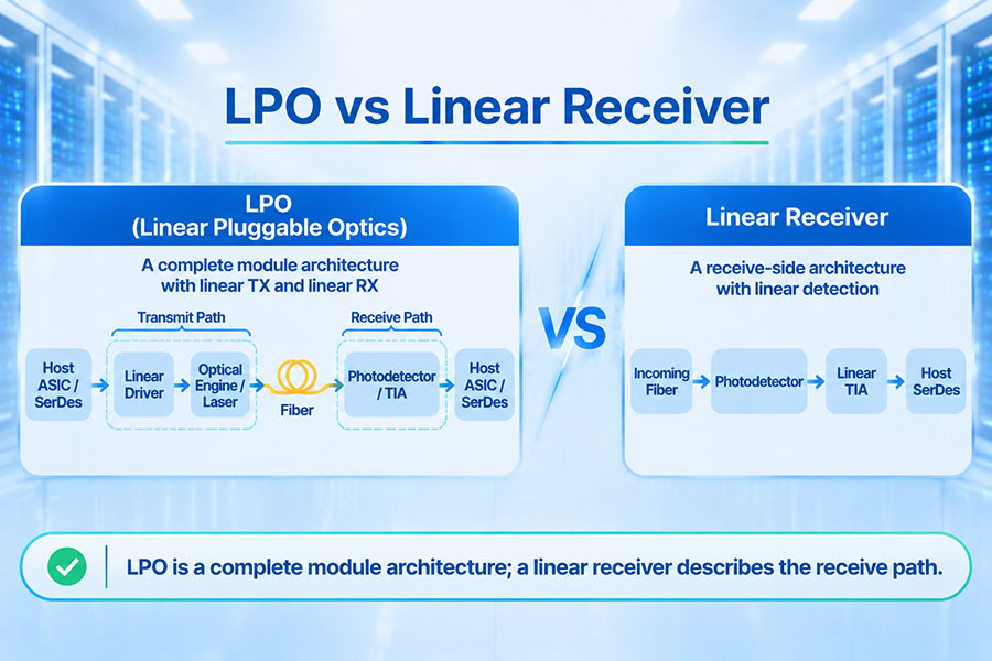
Linear Driver and DSP Driver describe transmitter-side implementation choices. LPO and LRO describe broader optical transceiver architectures that define how signal processing is distributed between the module and the host.
| Architecture | Transmit Side | Receive Side | General Processing Arrangement |
|---|---|---|---|
| Fully Retimed DSP Optics | DSP-based / retimed | DSP-based / retimed | Module performs substantial processing in both directions |
| LRO / RTLR | Retimed transmit | Linear receive | Transmit-side DSP or retiming retained; receive-side path is linear |
| LPO | Linear driver | Linear TIA | Host SerDes performs more of the electrical signal conditioning |
LRO is a half-retimed architecture. It retains transmit-side processing while reducing receiver-side module processing. LPO removes conventional module DSP retiming from both high-speed signal paths and relies more heavily on host SerDes capabilities.
A linear driver can therefore be used in an LPO transmitter, but the presence of a linear driver alone does not establish that an entire optical transceiver is LPO. The receive path, signal-processing allocation, and module architecture must also be considered.
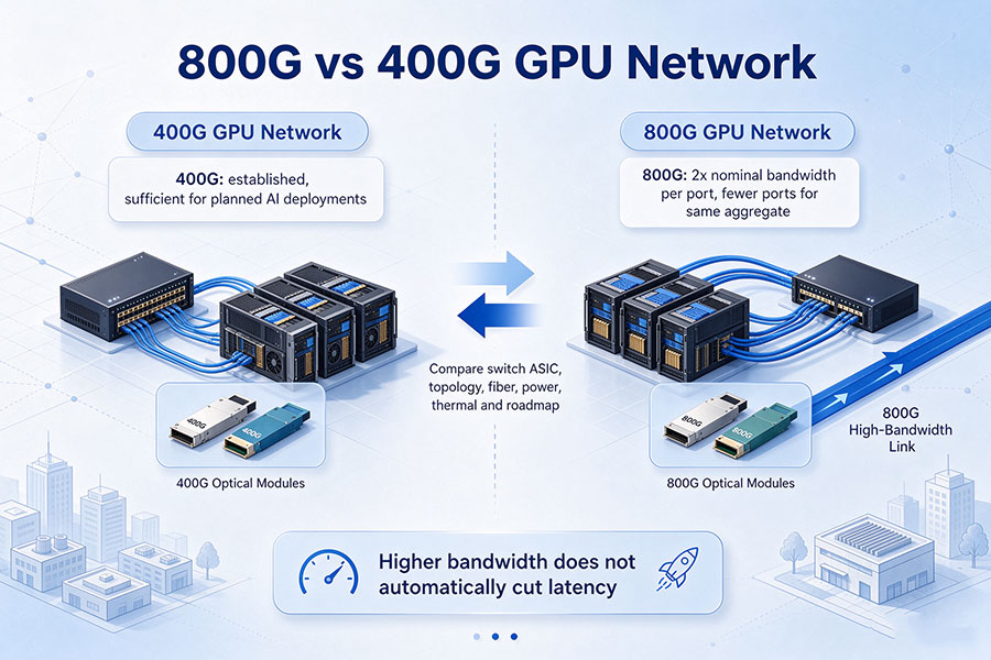
9. Linear Driver vs DSP Driver in 400G, 800G, and 1.6T Systems
Higher optical data rates increase the demands placed on transmitter bandwidth, electrical signal integrity, modulation quality, and host SerDes performance. The choice between linear and DSP-based transmit architectures becomes increasingly important as data center networks move toward 800G and 1.6T connectivity.
400G optical transmitters
Many 400G implementations use four approximately 100G-class electrical lanes, although the exact lane mapping and signaling depend on the interface. Linear-drive designs can reduce module processing overhead in suitable short-reach applications. DSP-based designs provide additional in-module signal-conditioning flexibility.
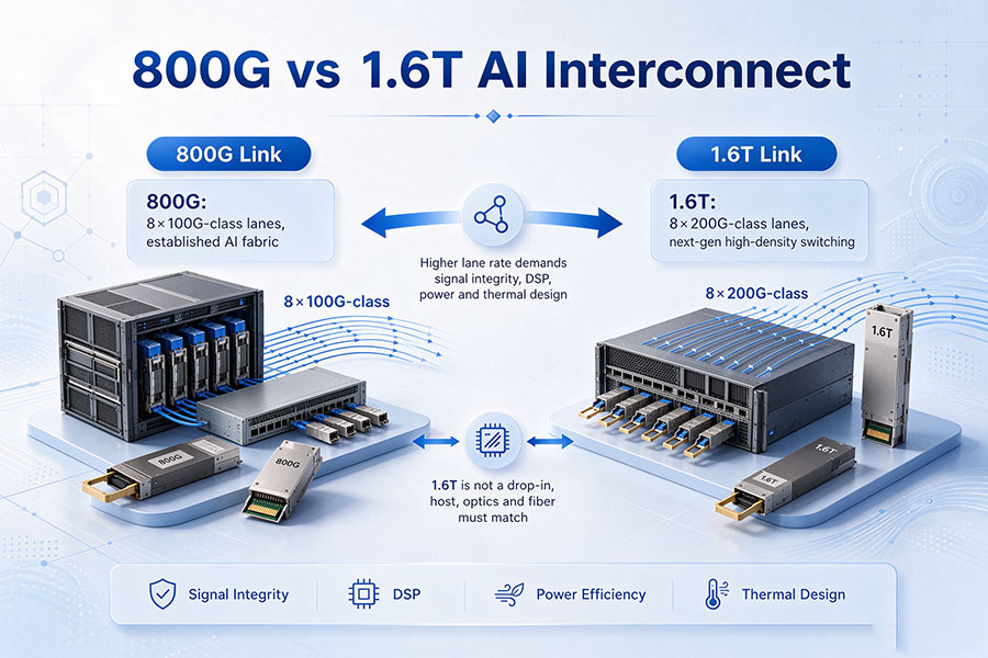
800G optical transmitters
800G optical modules commonly use eight approximately 100G-class electrical lanes. At this scale, the power and thermal benefits of reducing module DSP processing can become significant across a large switch port count. However, the host SerDes and electrical channel must support the required linear signal path.
1.6T optical transmitters
1.6T architectures commonly move toward eight approximately 200G-class electrical lanes. Higher lane rates make driver bandwidth, linearity, output swing, modulator response, and host signal integrity increasingly important.
Neither architecture is automatically better for every 1.6T application. The appropriate choice depends on the optical reach, modulation technology, host SerDes generation, electrical channel, power budget, and system-level performance targets.
10. Optical Modulator Compatibility and Transmitter Validation
Selecting a linear or DSP-based transmitter requires more than checking the module's nominal data rate. The driver must be compatible with the optical device, and the complete transmitter must meet the electrical and optical requirements of the link.
Important evaluation points include:
Driver bandwidth: Confirm that the driver supports the required modulation bandwidth and lane rate.
Output swing: Verify that the driver can provide the required electrical amplitude for the selected laser or modulator.
Linearity: Evaluate the driver's linear operating range and distortion characteristics under the specified conditions.
Host SerDes: Confirm transmit equalization, output swing, and electrical interface compatibility, especially for linear-drive modules.
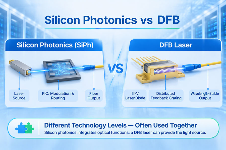
Optical device: Match the driver to the DML, EML, MZM, or other selected optical transmitter technology.
Signal quality: Measure optical eye characteristics, extinction ratio, jitter, and TDECQ where applicable.
Optical performance: Validate output power, wavelength, transmitter quality, and link budget.
Thermal behavior: Check module power and operating temperature under the intended airflow and system conditions.
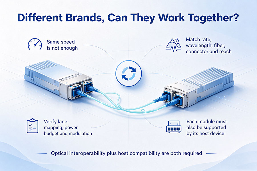
Interoperability: Test the complete host and module combination rather than relying on form factor or nominal speed alone.
11. C-LIGHT High-Speed Optical Connectivity
The choice of transmitter architecture is one part of a complete optical connectivity design. For 400G, 800G, and 1.6T networks, the optical module must also match the host platform, optical interface, fiber infrastructure, transmission distance, and thermal requirements.
C-LIGHT provides optical transceiver solutions for data center and telecommunications applications. The C-LIGHT Optical Transceiver portfolio provides a starting point for evaluating modules across different speeds and network requirements.
For high-speed AI and data center connectivity, selecting between DSP-based and linear-drive architectures requires attention to both the optical transmitter and the host electrical interface. The driver, modulator, SerDes, and complete channel must operate as a coordinated system.
Customers evaluating optical transceivers should confirm the required data rate, wavelength, optical reach, fiber type, connector, host compatibility, and power budget before deployment.
For optical transceiver selection, compatibility testing, and customized connectivity requirements, Contact C-LIGHT.
12. Conclusion
Linear drivers and DSP-based transmitter architectures differ mainly in where signal conditioning and digital processing take place. A linear driver amplifies and drives the optical modulator through an analog signal path, relying more heavily on host SerDes equalization. A DSP-based architecture performs additional digital processing inside the optical module before the signal reaches the analog modulator driver.
Linear-drive designs can reduce module power and processing latency, making them attractive for carefully engineered short-reach data center links. Their success depends on driver linearity, optical modulator characteristics, host SerDes capability, and electrical channel quality.
DSP-based transmitters provide greater in-module signal-conditioning flexibility and can compensate for selected electrical impairments. They remain important where additional processing and signal-control capabilities are required.
As 400G, 800G, and 1.6T optical networks evolve, the best architecture is determined by the complete link rather than the driver alone. Host compatibility, optical performance, module power, thermal design, and end-to-end signal integrity should all be evaluated together.
 >

 >
 >
 >
 >
 >
 >
 >