TEL:+86 132 6656 7067





High-speed optical transceivers depend on two closely related technologies: semiconductor materials that generate light and photonic platforms that manipulate optical signals. Indium phosphide (InP) has become an important material for lasers, electro-absorption modulators, and other active optical components. Silicon photonics (SiPh), meanwhile, provides a scalable platform for integrating waveguides, modulators, filters, and photodetectors.
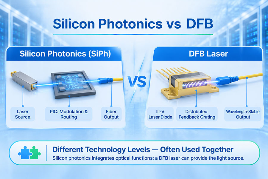
Although InP and silicon photonics are frequently discussed as competing optical technologies, they can also work together. An InP laser can supply continuous-wave light to a silicon photonic integrated circuit, where integrated modulators encode data and waveguides route the optical signals. This combination is increasingly relevant to high-density optical connectivity, including 400G, 800G, and emerging 1.6T systems.
1. What Is an InP Laser?
Indium phosphide (InP) is a III-V compound semiconductor with a direct bandgap. It is widely used in optical communication because its material properties support efficient light generation at important telecommunications wavelengths, particularly around the 1310 nm and 1550 nm regions.
InP is not limited to one laser structure. It can be used to manufacture several types of semiconductor lasers and integrated active photonic devices, depending on the required wavelength, output power, modulation method, and transmission application.
Common InP-based laser structures include:
DFB laser: A distributed feedback laser designed to provide stable, narrow-linewidth, single-mode emission. It is widely used in single-mode optical transceivers.
DBR laser: A distributed Bragg reflector laser that uses wavelength-selective reflectors and can support tunable or specialized laser configurations.
EML: An electro-absorption modulated laser that integrates a DFB laser section with an electro-absorption modulator.
DFB-MZ: A DFB laser combined with a Mach-Zehnder modulator in an integrated optical transmitter architecture.
Tunable laser: A laser designed to operate across a controlled wavelength range, useful in wavelength-selective optical systems.
InP can also support semiconductor optical amplifiers, photodetectors, and passive photonic structures. Its ability to combine light generation with other active optical functions makes it a significant material platform for integrated photonics.
2. What Is a Silicon Photonics Laser?
Silicon photonics is a photonic integration technology built around silicon-based optical circuits. It uses the properties of silicon and related materials to create compact optical waveguides, modulators, filters, and other photonic components.
The phrase Silicon Photonics Laser can be misleading if it suggests that conventional silicon itself is the primary light-generating material. Silicon has an indirect bandgap and is inefficient for conventional electrically pumped laser emission. Commercial silicon photonics systems therefore commonly use III-V semiconductor laser sources, including InP-based devices.
There are several ways to provide a laser source for a silicon photonic circuit:
External laser source: A separate laser supplies continuous-wave light to the silicon photonic chip through an optical connection.
Hybrid integration: An InP or other III-V laser chip is assembled with a silicon photonic chip in a shared package.
Heterogeneous integration: III-V gain material is bonded or otherwise integrated with the silicon photonic platform to create a more closely integrated light source.
Direct integration research: Researchers are developing methods to grow or integrate light-emitting materials on silicon, although manufacturing complexity and material compatibility remain important challenges.
Once light enters the silicon photonic circuit, integrated components can perform modulation, routing, filtering, and wavelength multiplexing. The resulting optical signals are then coupled to the fiber interface.
3. InP Laser vs Silicon Photonics: Core Differences
The two technologies differ in their material properties, optical functions, integration methods, and manufacturing approaches. InP has a strong position in active photonic components, while silicon photonics is particularly attractive for dense integration of passive and electro-optic functions.
| Technical Factor | InP Laser Platform | Silicon Photonics Platform |
|---|---|---|
| Technology category | III-V compound semiconductor material platform | Silicon-based photonic integration platform |
| Light generation | Direct semiconductor light generation | Usually relies on an external or integrated III-V laser source |
| Common wavelengths | 1310 nm and 1550 nm communication bands | Commonly designed for 1310 nm and 1550 nm systems |
| Laser structures | DFB, DBR, EML-based laser sections, and other structures | Laser source is usually a separate or integrated III-V device |
| Modulation | Direct modulation, EAM, and integrated MZ approaches | Commonly uses silicon MZMs or microring modulators |
| Passive waveguides | Available, but integration density and design depend on the InP process | Strong capability for compact, high-density waveguide circuits |
| Active optical functions | Lasers, amplifiers, modulators, and photodetectors can be integrated | Often combines silicon photonics with separate or integrated active materials |
| WDM integration | Possible through integrated active and passive structures | Well suited to compact wavelength multiplexers and demultiplexers |
| Manufacturing ecosystem | Specialized III-V semiconductor fabrication | Benefits from silicon wafer-processing infrastructure and photonic integration |
| Typical application focus | Laser sources and active optical transmitters | High-density photonic circuits and integrated optical engines |
These categories are not mutually exclusive. InP can form part of a silicon photonics product, and advanced InP PICs can also integrate passive optical functions. The comparison is most useful when it distinguishes the material platform from the complete optical system.
4. Light Generation: Direct Bandgap vs Indirect Bandgap
The underlying semiconductor physics explains why InP and silicon have different roles in optical communication.
InP has a direct bandgap. Electrons and holes can recombine efficiently while emitting photons, making it suitable for electrically pumped laser devices. This property supports the production of DFB lasers, tunable lasers, and other active optical components.
Silicon has an indirect bandgap. Its electronic band structure makes efficient conventional light emission much more difficult because the transition generally involves a momentum change. As a result, silicon photonics typically separates the light-generation function from the silicon-based optical routing and modulation functions.
| Material Property | InP | Silicon |
|---|---|---|
| Bandgap type | Direct | Indirect |
| Conventional laser emission | Efficient light generation is possible | Inefficient without additional structures or mechanisms |
| Optical gain | Suitable for active laser gain regions | Not normally used as the gain medium in conventional silicon photonics lasers |
| Typical role | Laser source and active photonic components | Waveguides, modulators, filters, and integrated optical routing |
This material difference is the fundamental reason why InP remains important to silicon photonics. Rather than replacing InP, silicon photonics often uses InP to provide the optical energy required by the integrated circuit.
5. InP DFB, EML, and Silicon Photonics Modulators
Modulation architecture has a major influence on transmitter performance. InP and silicon photonics can both support high-speed optical modulation, but their device structures and integration approaches are different.
InP DFB laser
A DFB laser generates light at a controlled wavelength using a distributed grating structure. Depending on the device and transmitter design, the laser can be directly modulated or used as a continuous-wave source for an external modulator.
InP EML
An EML combines a DFB laser with an electro-absorption modulator. The laser generates the optical carrier, while the modulator controls the transmitted optical intensity. This integration is useful for high-speed optical transmitters where compact packaging and controlled modulation performance are important.
Silicon photonics MZM
A silicon Mach-Zehnder modulator uses an interferometric structure to convert an electrical drive signal into changes in optical intensity or phase. It can be integrated with silicon waveguides and wavelength-routing components.
Silicon photonics microring modulator
A microring modulator uses a resonant optical structure to control transmission at a selected wavelength. Its compact footprint can support dense photonic integration, although wavelength and temperature sensitivity require careful control.
| Device | Operating Principle | Primary Function |
|---|---|---|
| InP DFB | Distributed feedback laser cavity | Stable optical carrier generation |
| InP EML | DFB laser combined with electro-absorption modulation | Integrated optical generation and intensity modulation |
| InP DFB-MZ | DFB laser combined with a Mach-Zehnder modulator | Optical generation and external-style modulation in an integrated device |
| Silicon MZM | Interferometric modulation in silicon waveguides | High-speed phase or intensity modulation |
| Silicon microring | Resonant wavelength-selective modulation | Compact modulation and wavelength-selective integration |
There is no universal winner across all modulation designs. The appropriate device depends on baud rate, extinction ratio, insertion loss, driver voltage, optical power budget, thermal stability, and the overall transmitter architecture.
6. External, Hybrid, and Heterogeneous Laser Integration
One of the most important development areas in silicon photonics is the integration of efficient laser sources. The goal is to combine the light-generation capability of III-V materials with the dense photonic integration of silicon.
Three integration approaches are commonly discussed.
External integration: The laser is physically separate from the silicon PIC. Optical coupling connects the source to the photonic circuit. This arrangement can simplify independent laser sourcing and thermal management, but adds optical interfaces and packaging requirements.
Hybrid integration: A separately fabricated InP laser is assembled with the silicon PIC. This can reduce the optical path between the source and photonic circuit while retaining separate fabrication processes.
Heterogeneous integration: III-V gain material is bonded or integrated with silicon so that laser and photonic functions can be combined more closely on a common platform.
Each approach involves trade-offs in alignment, coupling loss, thermal management, manufacturing yield, repairability, and production cost.
7. Optical Performance: Power, Linewidth, and Insertion Loss
Optical performance should be assessed at both the component and system levels. InP laser characteristics influence the quality of the optical carrier, while the silicon photonic circuit introduces its own waveguide, modulator, and coupling characteristics.
Important InP laser parameters include:
Output power: Determines the available optical power before downstream coupling and modulation losses.
Wavelength stability: Important for fixed-wavelength and WDM systems.
Linewidth: Relevant to coherent transmission and other applications sensitive to laser phase noise.
Relative intensity noise: Can influence receiver performance and signal quality.
Threshold current and efficiency: Affect laser power consumption and thermal design.
Important silicon photonics parameters include:
Waveguide propagation loss: Determines how much optical power is lost while light travels through the PIC.
Modulator insertion loss: Reduces optical power available at the transmitter output.
Extinction ratio: Indicates the separation between optical signal levels.
Coupling loss: Occurs at interfaces between the laser, PIC, and fiber.
Thermal sensitivity: Can affect wavelength alignment, resonator behavior, and modulator operating points.
In a complete transceiver, laser output power alone does not determine link performance. The optical budget must include laser coupling, modulator loss, multiplexing loss, fiber attenuation, connector loss, and receiver sensitivity.
8. Power Consumption and Thermal Management
InP and silicon photonics have different power-consumption profiles because they perform different functions. An InP laser consumes electrical power to generate optical energy. A silicon photonic circuit may require power for modulators, tuning elements, and thermal stabilization, in addition to its laser source and associated electronics.
Silicon photonics can reduce component count through integration, but it does not automatically guarantee lower system power. Some silicon modulators require electrical drive power or active thermal control. External laser architectures also need to account for the power consumed by the laser source and any associated distribution or stabilization circuits.
InP devices can integrate several active optical functions, potentially reducing the number of separate components. However, laser efficiency, modulator drive requirements, operating temperature, and package design all affect total power.
A fair comparison should use the same measurement boundary, such as total transmitter power or complete transceiver power, and should consider energy per bit rather than laser-only power.
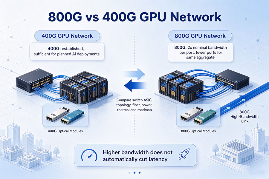
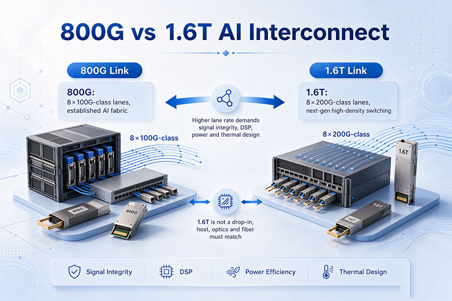
9. InP and Silicon Photonics in 400G, 800G, and 1.6T Optical Transceivers
Higher data rates require optical transmitters to support increasing lane speeds, channel counts, and integration density. Both InP and silicon photonics can contribute to these systems, but their roles vary by transceiver architecture.
| Optical System | Possible InP Role | Possible Silicon Photonics Role |
|---|---|---|
| 400G transceiver | DFB lasers, EMLs, and other active optical devices | Integrated modulators, waveguides, and WDM circuits |
| 800G transceiver | High-speed laser and modulator devices for optical lanes | Dense photonic integration and multi-channel optical routing |
| 1.6T transceiver | Laser sources and active optical components for higher-rate designs | Advanced PIC integration for high-density optical engines |
| Coherent optical module | Narrow-linewidth laser sources and integrated coherent photonic components | Photonic integration for modulators, routing, and coherent receiver functions |
These data rates do not belong exclusively to either technology. The final design may use InP-based EMLs, InP DFB lasers combined with silicon modulators, or other combinations of photonic components. Lane rate, modulation format, FEC, optical reach, and host electrical interface determine the complete implementation.
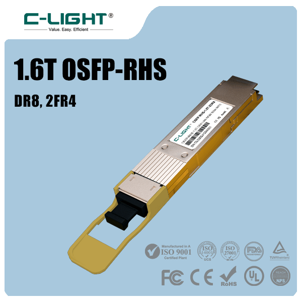
For optical connectivity across AI and data center networks, the C-LIGHT optical transceiver portfolio provides a relevant starting point for evaluating pluggable optical solutions. Product selection should be based on the specified wavelength, fiber type, reach, form factor, and host equipment compatibility rather than assuming a particular internal laser material.
10. Cost, Manufacturing, and Reliability
InP manufacturing uses specialized III-V semiconductor processes. These processes are well established for optical laser production but generally operate within a different manufacturing ecosystem from large-scale silicon CMOS fabrication.
Silicon photonics can benefit from silicon wafer-processing infrastructure and high-density integration. However, its manufacturing economics depend on PIC complexity, laser integration, packaging, fiber attachment, and test requirements.
| Evaluation Factor | InP Platform | Silicon Photonics Platform |
|---|---|---|
| Fabrication | Specialized III-V semiconductor processes | Silicon photonic wafer processes |
| Light-source integration | Native laser fabrication capability | Requires external, hybrid, or heterogeneous light-source integration in common designs |
| Integration strength | Active optical components | Dense passive and electro-optic photonic circuits |
| Packaging challenges | Laser coupling, thermal control, and active-device packaging | Laser-to-PIC coupling, fiber alignment, and PIC packaging |
| Reliability factors | Laser aging, wavelength stability, and temperature | Coupling stability, waveguide and modulator performance, and thermal control |
| Cost drivers | III-V wafer processing, device yield, and packaging | PIC fabrication, laser integration, optical assembly, and testing |
Neither platform has a universal cost or reliability advantage. High-volume production, device complexity, optical channel count, assembly method, and product lifetime requirements all influence the final result.
11. When to Choose InP or Silicon Photonics
The decision should be based on the optical functions required by the product. If the design needs a reliable semiconductor laser source or an integrated active transmitter, InP is a strong candidate. If the design needs dense optical routing, multiple integrated modulators, or wavelength multiplexing, silicon photonics may provide a more suitable integration platform.
Consider InP when: The design prioritizes laser generation, high optical gain, integrated active devices, or a compact EML-based transmitter.
Consider silicon photonics when: The design prioritizes dense waveguide integration, multiple optical functions on a PIC, or scalable WDM architectures.
Consider an InP-plus-SiPh architecture when: The product needs InP laser performance together with silicon photonic routing, modulation, or wavelength multiplexing.
Before selecting an optical engine or transceiver, engineering teams should verify:
Target data rate and optical lane configuration
Operating wavelength and wavelength stability
Laser output power and receiver sensitivity
Modulation format and bandwidth
Optical insertion loss and link budget
Single-mode fiber type and required transmission distance
Power consumption and thermal operating limits
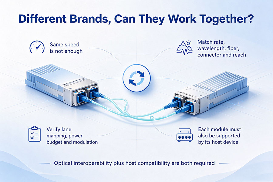
Packaging, fiber coupling, and equipment compatibility
12. Conclusion
InP and silicon photonics are complementary technologies with different strengths. InP provides an efficient semiconductor platform for generating light and integrating active optical devices. Silicon photonics provides a high-density platform for optical waveguides, modulators, filters, and other integrated photonic functions.
For high-speed optical transceivers, InP can serve as the laser source, while silicon photonics can perform modulation and optical routing. Hybrid and heterogeneous integration bring these capabilities together in compact optical engines. As 400G, 800G, and 1.6T connectivity develops, the most suitable architecture will depend on optical performance, power consumption, packaging, manufacturing yield, and system-level cost.
The central engineering decision is therefore not simply InP versus silicon photonics. It is how to combine light generation and photonic integration to meet the requirements of the complete optical link.
Looking for optical transceiver solutions for your network?
C-LIGHT supports optical connectivity requirements across data center, telecommunications, and high-speed networking applications. Share your target data rate, wavelength, transmission distance, and equipment platform to discuss a suitable solution.
 >

 >
 >
 >
 >
 >
 >
 >