TEL:+86 132 6656 7067




Silicon Photonics and Indium Phosphide (InP) are two important technologies used in modern optical communication systems. Both can support high-speed optical transmission, but they approach the problem from different technological directions.
Silicon Photonics is primarily a photonic integration platform in which optical waveguides, modulators, multiplexers, splitters, couplers, and other photonic functions can be integrated onto a silicon photonic integrated circuit (PIC). InP is a semiconductor material platform widely used for active photonic devices such as lasers, electro-absorption modulators, photodiodes, and integrated laser-modulator structures.
The distinction is important because Silicon Photonics and InP can also be used together. A silicon photonics transceiver may use an InP continuous-wave laser as its light source, while the modulation and wavelength-routing functions are implemented on a silicon photonic PIC. Therefore, the industry does not always treat SiPh and InP as mutually exclusive technologies.
1. What Is Silicon Photonics?
Silicon Photonics, commonly abbreviated as SiPh, uses silicon-based photonic integrated circuits to guide, modulate, combine, split, and detect optical signals.
A silicon photonic PIC can integrate multiple passive and active photonic functions into a relatively compact structure. Typical elements include optical waveguides, Mach-Zehnder modulators, resonators, splitters, couplers, wavelength multiplexers, demultiplexers, and photodetection structures.
The ability to integrate multiple optical functions on one PIC is one of the main characteristics of silicon photonics.
2. What Is InP?
InP stands for Indium Phosphide. It is a III-V semiconductor material widely used in optical communication devices.
InP is particularly important for active photonic components because it can be used to manufacture semiconductor lasers and other electro-optical devices. In optical communications, InP-based devices include distributed feedback (DFB) lasers, electro-absorption modulated lasers (EMLs), differential EMLs, continuous-wave lasers, modulators, and photodiodes.
InP technology can also support integrated laser and modulator structures, allowing several active optical functions to be implemented within a single semiconductor platform.
3. Silicon Photonics vs InP: Basic Difference
| Feature | Silicon Photonics | InP-Based Technology |
|---|---|---|
| Primary Role | Photonic integration platform | Active semiconductor photonic platform |
| Core Material | Silicon | Indium Phosphide |
| Waveguide Integration | Highly suitable | Suitable |
| Laser Generation | Usually requires hybrid or external III-V laser integration | Native platform for semiconductor lasers |
| Modulation | Integrated photonic modulators | EML, D-EML, DFB-MZ and other active structures |
| WDM Integration | Highly suitable | Possible through integrated or discrete structures |
| Integration Approach | High photonic integration | Strong active-device integration |
| Typical Applications | Data center, WDM, AI and high-density optical systems | Data center, telecom, high-speed lasers and optical engines |
The comparison should therefore focus on the complete photonic architecture rather than assuming that one material automatically replaces the other.
4. Why Is Silicon Photonics Different from InP?
The fundamental difference comes from the functions that each platform performs particularly well.
Silicon provides an effective platform for low-loss optical waveguides and dense photonic integration. InP is particularly useful for active light generation and electro-optical devices.
This leads to different product architectures. A Silicon Photonics module can integrate modulation and optical routing on silicon while using a separate InP laser. An InP-based module can integrate the laser and modulator more directly in the III-V material platform.
5. Silicon Photonics PIC Architecture
A Silicon Photonics PIC acts as the optical integration layer inside a transceiver.
Electrical data can be applied to an integrated modulator, where the electrical signal controls the optical carrier. The modulated optical signal then travels through silicon waveguides to multiplexers, couplers, or the fiber interface.
On the receiver side, the PIC can route incoming optical signals to integrated photodetection structures or to separate receiver components.
This architecture allows several optical channels to share a common photonic platform.
6. InP Active Photonic Architecture
InP-based photonic devices can combine active optical functions in a semiconductor platform.
An InP EML, for example, combines a distributed-feedback laser with an electro-absorption modulator. This creates a compact optical transmitter capable of high-speed modulation.
Other InP architectures can integrate a continuous-wave laser with a Mach-Zehnder modulator, such as an InP DFB-MZ device, for higher-speed optical transmission.
These architectures are particularly relevant when high optical output, high modulation bandwidth, and long-reach single-mode transmission are required.
7. Light Generation
One of the most important differences between SiPh and InP is the generation of light.
Silicon photonics itself is not normally the primary light-generating material. Silicon photonic modules often require an external or hybrid-integrated III-V laser source.
InP is directly suited to semiconductor laser generation, so an InP-based architecture can place the light source and modulation components much closer together.
In practical products, an InP laser can therefore serve as the light source for a silicon photonics PIC.
8. InP Lasers in Silicon Photonics
The relationship between SiPh and InP is especially clear in hybrid architectures.
An InP continuous-wave laser can provide a stable optical carrier to a silicon photonic modulator. The silicon PIC then performs the modulation, optical routing, and wavelength multiplexing functions.
This architecture combines the laser-generation capability of InP with the integration capability of silicon photonics.
Coherent currently lists high-power InP CW lasers specifically for silicon photonics transceivers and CPO applications, illustrating that InP and SiPh can form a combined optical architecture rather than competing independently.
9. Silicon Photonics Modulators
Silicon photonics can implement high-speed modulators directly on the PIC.
Mach-Zehnder modulators are commonly used because they can provide broadband optical modulation suitable for high-speed data transmission.
The modulator changes the optical carrier according to the electrical input signal. Because multiple modulator channels can be integrated on the same PIC, silicon photonics can support dense multi-channel optical architectures.
10. InP EML Technology
EML is one of the most important InP-based technologies for high-speed optical transceivers.
An EML combines a DFB laser with an electro-absorption modulator. The laser generates the optical carrier, while the electro-absorption section modulates the optical signal.
InP EMLs are widely used for single-mode optical transmission and can support high per-lane data rates.
Coherent's current InP portfolio includes 200G EML technology for 1.6T transceiver applications and differential EML technology targeting 400G-per-lane optical transmission for emerging higher-speed systems.
11. Silicon Photonics vs InP Modulation
| Parameter | Silicon Photonics | InP-Based Modulation |
|---|---|---|
| Typical Modulator | Silicon photonic Mach-Zehnder modulator | Electro-absorption modulator, Mach-Zehnder modulator |
| Laser Relationship | Often external or hybrid-integrated | Can be integrated with modulator |
| WDM Integration | Strong | Possible |
| Integration Style | PIC-based | Active III-V semiconductor integration |
| Common High-Speed Use | 400G / 800G / 1.6T | 400G / 800G / 1.6T and emerging higher-speed systems |
12. Silicon Photonics and WDM
Silicon photonics is particularly suitable for wavelength-division multiplexing because multiple wavelength-routing structures can be integrated directly onto the PIC.
Optical multiplexers and demultiplexers can combine several wavelengths into one fiber and separate them again at the receiver.
This is useful for architectures such as 400G FR4, 800G FR4, and other WDM-based optical systems.
13. InP and WDM
InP devices can also be used in wavelength-multiplexed systems. InP lasers can provide individual wavelength channels, while multiplexing functions can be implemented using separate optical components or integrated structures.
In some architectures, InP provides the laser and modulator while another photonic platform handles wavelength multiplexing.
This division of functions allows designers to select different technologies for different parts of the optical path.
14. Receiver Technology
Both Silicon Photonics and InP can be used in receiver architectures, but the implementation differs.
Silicon photonics can integrate optical routing and photodetection structures into a PIC. Germanium photodetectors are commonly used with silicon photonic platforms because germanium provides suitable optical absorption in important telecom and data center wavelength bands.
InP-based receivers can use high-speed photodiodes and receiver structures fabricated from III-V semiconductor technologies.
In both cases, the photodetector is normally paired with electrical receiver circuitry such as a TIA.
15. Silicon Photonics and Photodetectors
A silicon photonics receiver can combine waveguides, optical couplers, wavelength demultiplexers, and photodetectors within a compact PIC architecture.
This makes it possible to create multi-channel receiver structures with a relatively high level of optical integration.
Integrated receiver structures can be particularly useful for WDM modules where several optical wavelengths need to be separated and detected.
16. InP Photodetectors
InP-based photonic technology can provide high-speed photodetectors for optical communications.
PIN and other photodetection structures can be optimized for the required wavelength, bandwidth, sensitivity, and optical power range.
Coherent's 2026 InP portfolio includes 200G and 400G photodiodes for next-generation optical communication applications.
17. 400G Applications
Both Silicon Photonics and InP technologies can support 400G optical transceivers.
Silicon photonics can integrate multi-channel modulation and WDM functions into a compact PIC. InP-based solutions can use EML or other active photonic devices to provide the optical transmit path.
The specific architecture depends on the optical reach, optical channel count, wavelength plan, power budget, and module design.
18. 800G Applications
800G optical modules increase the requirements for optical integration and per-lane bandwidth.
Silicon photonics can integrate multiple optical channels and wavelength functions while supporting high-density optical engine architectures.
InP EML technology can provide high-speed optical lanes for 800G modules. Coherent has demonstrated 800G DR8 solutions based on both silicon photonics and InP EML technologies, showing that different optical architectures can address the same aggregate bandwidth.
19. 1.6T Applications
1.6T transceivers require eight 200G-class electrical or optical lanes in many architectures, placing substantial requirements on optical transmitters, receivers, modulators, and packaging.
Silicon photonics can integrate multiple 200G-class optical channels into a compact PIC-based architecture.
InP technology can provide 200G EMLs, high-power CW lasers, and other active optical components for 1.6T systems.
Current industry demonstrations include 1.6T transceivers based on silicon photonics, InP EML, and other optical technologies.
20. 200G-per-Lane Optical Technology
As the industry moves toward 1.6T and beyond, 200G-per-lane optical technology becomes increasingly important.
Silicon photonics can use high-speed Mach-Zehnder modulators for 200G-class optical lanes.
InP can use high-speed EMLs or DFB-MZ architectures to generate and modulate high-speed optical signals.
Both approaches require careful optimization of optical modulation bandwidth, linearity, insertion loss, drive voltage, thermal behavior, and packaging.
21. 400G-per-Lane Development
Future optical architectures are moving beyond 200G-per-lane operation toward 400G-per-lane technologies.
In 2026, Coherent reported differential EML technology targeting 400G-per-lane performance for emerging 3.2T and higher-speed pluggable applications.
Silicon photonics is also being developed for higher-speed modulator architectures, although the exact device technology and system implementation vary between manufacturers.
22. Manufacturing and Wafer Processing
Silicon photonics benefits from compatibility with semiconductor-style wafer processing.
Multiple PICs can be fabricated across a wafer, followed by wafer-level optical and electrical testing before final packaging.
This manufacturing approach can support high-volume production and can reduce some of the individual alignment operations associated with discrete optical assemblies.
However, the final module still requires laser integration, fiber coupling, electrical connection, thermal management, and package assembly.
23. InP Manufacturing
InP devices are also manufactured using wafer-based semiconductor processes, but the material platform and fabrication processes differ from those used for silicon photonics.
InP manufacturing is particularly suited to active optical components such as lasers, EMLs, modulators, and photodiodes.
InP device manufacturing can provide high levels of active photonic integration, while silicon photonics provides strong integration for passive routing and multi-channel photonic functions.
24. Optical Coupling
Optical coupling is an important manufacturing consideration for both platforms.
In a silicon photonics module, light must be coupled between the laser and PIC and between the PIC and optical fiber.
In an InP-based module, laser and modulator structures can be integrated more directly, but fiber coupling and package alignment are still required.
Advanced packaging methods such as edge coupling, grating coupling, active alignment, and passive alignment can be used depending on the architecture.
25. Packaging
Silicon photonics packaging is a major part of system performance because the PIC, laser, fiber interface, electrical drivers, and thermal structures must operate together.
InP packaging must similarly control optical alignment, electrical parasitics, laser temperature, modulator performance, and fiber coupling.
At 800G and 1.6T, packaging performance becomes increasingly important because small parasitic effects can influence high-speed electrical and optical performance.
26. Thermal Management
Thermal management is important for both Silicon Photonics and InP technologies.
Laser efficiency, wavelength, modulator characteristics, photodetector response, and electronic performance can all vary with temperature.
In a silicon photonics module, the external or hybrid-integrated laser can be a major thermal source. In an InP module, the laser and modulator may be integrated closely, creating a tightly coupled thermal environment.
For high-speed modules, the optical engine, DSP, drivers, TIAs, and host system must all be considered as part of the thermal design.
27. Power Consumption
Power consumption depends on the complete optical module rather than the material platform alone.
Silicon photonics can reduce power in some architectures by integrating multiple optical functions and shortening optical paths, while high-speed integrated modulators can also reduce the number of discrete optical components.
InP can provide efficient active optical components, including lasers and EMLs, and can reduce some packaging complexity by integrating multiple active functions.
The total module power still depends on DSP, driver, TIA, laser, modulator, cooling, and electrical interface architecture.
28. Signal Integrity
High-speed signal integrity is a critical issue for both technologies.
Silicon photonics can reduce some electrical complexity by integrating optical modulation closer to the optical engine, but the electrical connection to the PIC and laser still requires careful design.
InP EML and related active devices must also maintain high-speed electrical and optical performance under demanding modulation conditions.
At 200G-per-lane and higher speeds, package parasitics, electrical bandwidth, impedance, crosstalk, and drive conditions become major design considerations.
29. Optical Reach
Neither Silicon Photonics nor InP automatically determines the transmission distance of a transceiver.
Reach depends on the complete optical architecture, including laser output, modulation technology, wavelength, fiber type, receiver sensitivity, optical link budget, dispersion, and signal processing.
Both technologies can be used for short, medium, and longer optical links when combined with the appropriate optical components and system architecture.
30. Silicon Photonics vs InP: Key Differences
| Parameter | Silicon Photonics | InP |
|---|---|---|
| Technology Type | Photonic integration platform | III-V semiconductor material platform |
| Waveguides | Strong integration capability | Available through semiconductor photonics structures |
| Light Source | Usually hybrid or external III-V laser | Native semiconductor laser platform |
| Modulator | Silicon photonic MZM and related devices | EML, D-EML, DFB-MZ and other active structures |
| WDM | Highly suitable for PIC integration | Can be implemented with active and passive structures |
| Integration | High passive and photonic integration | High active photonic integration |
| Manufacturing | Strong compatibility with CMOS-style wafer processing | Dedicated III-V semiconductor manufacturing |
| Typical High-Speed Use | 400G / 800G / 1.6T and beyond | 400G / 800G / 1.6T and beyond |
| Relationship | Can use InP laser technology | Can be integrated with silicon photonics |
31. Silicon Photonics and InP Can Work Together
It is inaccurate to assume that a transceiver must use either Silicon Photonics or InP exclusively.
A hybrid architecture can use an InP CW laser as the optical source and a silicon photonic PIC for modulation, wavelength multiplexing, routing, and coupling.
This division of functions allows each technology to perform the optical tasks for which it is well suited.
Current commercial and demonstration platforms provide multiple examples of this combined approach, particularly in high-speed data center optical transceivers.
32. Silicon Photonics vs InP in AI Data Centers
AI data centers require increasing bandwidth between GPUs, accelerators, switches, and storage systems.
As optical links move to 800G and 1.6T, the optical engine must support higher per-lane bandwidth while maintaining manageable power and thermal characteristics.
Silicon photonics provides a high-integration path for multi-channel optical engines, while InP provides high-speed lasers, EMLs, photodiodes, and other active devices.
The two technologies are therefore both relevant to AI optical interconnects and can also be combined in the same transceiver.
33. Silicon Photonics vs InP for Optical Transceivers
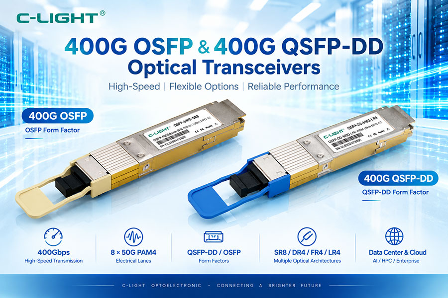
For pluggable transceivers, silicon photonics can provide an integrated PIC inside a conventional module package such as QSFP-DD or OSFP.
InP devices can be used inside the same form factors as lasers, EMLs, photodiodes, and other optical components.
Therefore, the form factor does not determine whether the module uses Silicon Photonics or InP. The optical architecture inside the module determines the underlying technology.
34. Silicon Photonics vs InP for CPO
Both Silicon Photonics and InP technologies can be used in highly integrated optical architectures such as Co-Packaged Optics.
Silicon photonics is useful for integrating optical routing and modulation close to the switch ASIC, while InP can provide the high-power laser source or other active optical components.
This makes hybrid SiPh and InP architectures relevant to CPO as well as pluggable optics.
35. Cost and Manufacturing Considerations
Cost depends on manufacturing volume, device complexity, packaging, laser integration, testing, yield, and supply chain rather than the material platform alone.
Silicon photonics can benefit from wafer-scale manufacturing and high levels of optical integration.
InP can provide integrated active optical functions and has a mature manufacturing ecosystem for lasers, EMLs, and photodetectors.
The final module cost therefore depends on the complete production flow and the target optical performance.
36. Reliability Considerations
Reliability must be evaluated at the complete module level.
Silicon photonics can reduce the number of discrete optical interfaces in some architectures, but laser coupling, fiber attachment, PIC packaging, thermal cycling, and electrical connections still need qualification.
InP devices also require control of laser degradation, thermal behavior, packaging stress, fiber alignment, and electrical performance over the specified operating range.
Both technologies require appropriate reliability testing and qualification for the intended network environment.
37. Testing and Qualification
Silicon photonic PICs can be tested at wafer level before final module assembly. Optical insertion loss, modulation response, wavelength characteristics, and other parameters can be evaluated before packaging.
InP devices can also be electrically and optically tested at the wafer or device level before integration into optical modules.
Final transceiver qualification still requires complete-module testing, including optical power, receiver sensitivity, BER, temperature performance, electrical characteristics, and interoperability.
38. Future Development
Both Silicon Photonics and InP are continuing to evolve with the growth of AI and high-speed data center networks.
Silicon photonics is moving toward higher-speed modulators, lower-loss PICs, more efficient laser integration, and higher levels of optical-electrical integration.
InP technology is advancing toward higher-speed EMLs, differential EMLs, high-power CW lasers, DFB-MZ devices, and high-speed photodiodes.
Current 2026 developments show these technologies advancing in parallel. Coherent is presenting InP solutions for 1.6T and emerging 3.2T systems, while silicon photonics platforms are also progressing toward 1.6T and beyond.
39. Conclusion
Silicon Photonics and InP represent two important technologies in high-speed optical communication, but they should not be treated as identical categories.
Silicon Photonics is primarily an integrated photonic platform that is particularly suitable for optical routing, modulation, WDM, and multi-channel integration. InP is a III-V semiconductor platform that is particularly important for active optical devices such as lasers, EMLs, modulators, and photodetectors.
In many modern optical transceivers, the two technologies work together. An InP laser can provide the optical carrier for a silicon photonic PIC, while the PIC performs modulation and wavelength-routing functions.
As optical networking moves from 400G to 800G, 1.6T, and higher bandwidth levels, the choice of optical technology will depend on link distance, laser power, modulation bandwidth, integration, power consumption, thermal design, packaging, manufacturing, and system architecture.
Rather than viewing Silicon Photonics and InP as mutually exclusive technologies, it is more accurate to view them as complementary platforms that can be combined to build high-performance optical transceivers and optical engines.
 >
>

 >
>
 >
>
 >
>
 >
>
 >
>
 >
>
 >
>