TEL:+86 132 6656 7067




EML and silicon photonics are two technologies for generating and modulating light in an optical transceiver. EML stands for Electro-absorption Modulated Laser. It is a discrete component built on Indium Phosphide, with a distributed feedback laser and an electro-absorption modulator integrated on the same chip. Silicon photonics is a platform technology that integrates modulators, waveguides, and photodetectors on a silicon substrate using CMOS-compatible manufacturing processes.
The two are often presented as competing approaches for high-speed optical engines. In practice, they occupy different positions in the transceiver supply chain. EML is a component: a laser chip that is packaged inside a module. Silicon photonics is a platform: a manufacturing approach that can produce an entire optical engine on a single die or chipset. The comparison is not between two equivalent components but between a mature discrete laser technology and an emerging integration platform.
Both are used in 400G, 800G, and 1.6T transceivers. Both support PAM4 modulation at 100G and 200G per lane. Both are being deployed in AI data centers at scale. The differences lie in the material system, the level of integration, the manufacturing economics, the power consumption, and the path each technology takes toward co-packaged optics.
1. What Is EML?
An EML is a monolithic chip that combines a distributed feedback laser with an electro-absorption modulator. The DFB section generates continuous-wave light at a stable wavelength, and the EAM section modulates that light by applying a voltage that changes the material's absorption coefficient. The two sections are fabricated on the same Indium Phosphide substrate and coupled through an integrated waveguide.
The advantage of EML is that it integrates the laser and the modulator on one chip, eliminating the need for external modulation. This reduces the optical loss and the packaging complexity compared to a discrete laser followed by a separate modulator. EMLs are the workhorse of 100G and 200G per lane direct-detect optics, and they are used in LR4, ER4, and other LAN-WDM interfaces at 400G and 800G.
1.1 EML Characteristics
Material system: Indium Phosphide.
Integration level: Laser and modulator on one chip.
Wavelength: 1310 nm or 1550 nm, depending on the design.
Modulation: Electro-absorption, directly driven by a PAM4 signal.
Chirp: Low, because the modulator is separate from the laser gain section.
Extinction ratio: High, typically 8 to 10 dB.
Manufacturing: Mature, high-volume, with established supply chains.
Typical application: 100G and 200G per lane direct-detect optics.
2. What Is Silicon Photonics?
Silicon photonics is a platform that uses silicon and silicon-compatible materials to build optical components on a chip. Silicon itself is not an efficient light emitter, so silicon photonics integrates external lasers—either as discrete components or as bonded III-V chips—and uses silicon for the passive and active functions: waveguides, modulators, multiplexers, and photodetectors.
The modulator in a silicon photonics platform is typically a Mach-Zehnder interferometer that uses the free-carrier dispersion effect to change the refractive index of silicon and modulate the phase of the light. The interference between the two arms converts the phase modulation into amplitude modulation. Silicon photonics can also integrate germanium photodetectors, which are compatible with CMOS processing.
2.1 Silicon Photonics Characteristics
Material system: Silicon and silicon-compatible materials.
Integration level: Waveguides, modulators, multiplexers, and photodetectors on one die.
Laser source: External or bonded III-V laser.
Modulation: Mach-Zehnder or ring resonator, driven by a PAM4 signal.
Chirp: Low, because the modulator is separate from the laser.
Extinction ratio: Moderate to high, depending on the design.
Manufacturing: CMOS-compatible, with the potential for high-volume wafer-scale production.
Typical application: 400G, 800G, and 1.6T optical engines, including co-packaged optics.
3. Material System and Light Generation
The fundamental difference between EML and silicon photonics is the material system. EML uses Indium Phosphide, a direct-bandgap semiconductor that emits light efficiently. Silicon is an indirect-bandgap material and does not emit light efficiently, so silicon photonics must integrate an external laser source.
This difference shapes the manufacturing economics and the integration path of each technology. EML is a discrete component that is fabricated on III-V wafers and packaged into modules. Silicon photonics is a platform that can integrate most of the optical engine on a silicon die, with the laser as the remaining discrete component. The laser can be placed outside the package, coupled into the silicon photonics chip through a fiber or a grating coupler, or bonded directly onto the silicon die as a III-V chip.
| Parameter | EML | Silicon Photonics |
|---|---|---|
| Material System | Indium Phosphide | Silicon with III-V laser |
| Light Generation | On-chip DFB laser | External or bonded III-V laser |
| Modulator Material | Indium Phosphide | Silicon |
| Waveguide Material | Indium Phosphide | Silicon |
| Photodetector Material | Indium Phosphide | Germanium on silicon |
4. Integration Level and Packaging
EML integrates two functions—laser and modulator—on one chip. The rest of the optical engine, including the multiplexer, the photodiodes, and the coupling optics, is packaged separately. A 400GBASE-LR4 module using EMLs contains four EML chips, a LAN-WDM multiplexer, a demultiplexer, and four photodiodes, all assembled in a hermetic or semi-hermetic package.
Silicon photonics integrates the modulators, waveguides, multiplexers, and photodetectors on a single silicon die. The laser remains a separate component, but the rest of the optical engine is on-chip. This reduces the number of discrete components, the number of optical alignments, and the packaging complexity. A silicon photonics-based 400G module may contain one silicon photonics die and one or more laser sources, rather than four separate EML chips and a discrete multiplexer.
| Parameter | EML | Silicon Photonics |
|---|---|---|
| Laser Integration | On-chip | External or bonded |
| Modulator Integration | On-chip | On-chip |
| Multiplexer Integration | Discrete | On-chip |
| Photodetector Integration | Discrete | On-chip |
| Component Count | Higher | Lower |
| Packaging Complexity | Higher | Lower |
| Optical Alignment Steps | More | Fewer |
5. Modulation and Signal Quality
EML uses electro-absorption modulation, which changes the absorption of the material by applying a voltage. The modulator section is separate from the laser gain section, which gives the EML low chirp and high extinction ratio. The modulation bandwidth of an EML is limited by the carrier dynamics in the electro-absorption material, but modern EMLs support 100G and 200G PAM4 per lane.
Silicon photonics uses Mach-Zehnder or ring resonator modulators, which change the refractive index of silicon by injecting or depleting free carriers. The modulation bandwidth is determined by the carrier lifetime and the device geometry. Modern silicon photonics modulators support 100G and 200G PAM4 per lane, and research devices have demonstrated higher speeds.
The signal quality of both technologies is sufficient for 400G, 800G, and 1.6T interfaces. The choice between them is not driven by modulation performance but by integration, manufacturing, and cost.
| Parameter | EML | Silicon Photonics |
|---|---|---|
| Modulation Mechanism | Electro-absorption | Free-carrier dispersion |
| Modulator Type | EAM | Mach-Zehnder or ring |
| Chirp | Low | Low |
| Extinction Ratio | 8–10 dB | 6–10 dB |
| Per-Lane Rate | 100G–200G PAM4 | 100G–200G PAM4 |
| Modulation Bandwidth | Limited by carrier dynamics | Limited by carrier lifetime and device geometry |
6. Power Consumption
EML power consumption is dominated by the laser drive current and the modulator bias. The DFB laser in an EML operates at a constant output power, and the modulator modulates that power. The laser consumes most of the power, and the modulator consumes a smaller amount for the bias and the RF drive.
Silicon photonics power consumption is also dominated by the laser, but the modulator consumes additional power for the free-carrier injection or depletion. Mach-Zehnder modulators have a relatively high drive voltage, while ring resonators have a lower drive voltage but require temperature stabilization. The total power consumption of a silicon photonics optical engine depends on the modulator design and the laser source.
At the module level, the power consumption of EML-based and silicon photonics-based transceivers is similar. Both are in the range of 10 to 25 watts for 400G and 800G modules, depending on the reach and the DSP. The choice between them is not driven by power consumption alone.
| Parameter | EML | Silicon Photonics |
|---|---|---|
| Dominant Power Consumer | Laser and modulator bias | Laser and modulator drive |
| Modulator Drive Voltage | Moderate | Higher for Mach-Zehnder |
| Temperature Stabilization | Required for wavelength | Required for ring resonators |
| Module Power (400G) | 10–16 W | 10–16 W |
| Module Power (800G) | 14–24 W | 14–24 W |
7. Manufacturing and Cost
EML manufacturing is based on Indium Phosphide wafer processing, which is a specialized and relatively expensive process compared to silicon CMOS. The III-V wafer size is smaller than silicon wafers, and the processing equipment is less standardized. However, EML manufacturing is mature, with decades of experience and established supply chains.
Silicon photonics manufacturing is based on CMOS-compatible processes, which can leverage the enormous scale and standardization of the silicon industry. Silicon wafers are larger, the processing equipment is more standardized, and the potential for wafer-scale testing and packaging is higher. The challenge is that silicon photonics still requires a III-V laser source, which must be integrated or coupled to the silicon die.
The cost comparison depends on the volume and the integration level. At low volumes, EML may be cheaper because the supply chain is mature and the components are available off the shelf. At high volumes, silicon photonics has the potential to be cheaper because the CMOS-compatible manufacturing can achieve lower cost per die and higher integration.
| Parameter | EML | Silicon Photonics |
|---|---|---|
| Wafer Material | Indium Phosphide | Silicon |
| Wafer Size | Smaller | Larger |
| Process Standardization | Specialized | CMOS-compatible |
| Supply Chain Maturity | High | Growing |
| Volume Cost | Moderate | Lower potential at high volume |
| Integration Level | Lower | Higher |
8. Application Scenarios
EML is used in direct-detect PAM4 transceivers from 100G to 800G, including LR4, ER4, and other LAN-WDM interfaces. It is the standard component for 100G and 200G per lane direct-detect optics, and it is deployed in large volumes in data center and telecom networks.
Silicon photonics is used in 400G, 800G, and 1.6T transceivers, including direct-detect and coherent interfaces. It is also the enabling platform for co-packaged optics, where the optical engine is integrated into the switch package. Silicon photonics is used in DR4, FR4, LR4, and coherent ZR modules, and it is being evaluated for co-packaged optics in AI data centers.
| Application | EML | Silicon Photonics |
|---|---|---|
| 100G LR4 | Primary | Possible |
| 400G LR4 | Primary | Growing |
| 400G FR4 | Primary | Growing |
| 800G LR4 | Primary | Growing |
| 400ZR | Not typical | Primary |
| Co-Packaged Optics | Not typical | Primary platform |
9. Path to Co-Packaged Optics
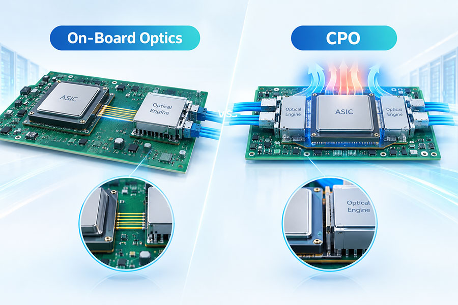
Co-packaged optics integrates the optical engine with the switch ASIC in the same package. This eliminates the pluggable module and the electrical interface between the module and the switch, reducing power consumption and improving signal integrity. The optical engine must be small, low-power, and compatible with the switch package's thermal and mechanical constraints.
Silicon photonics is the primary platform for co-packaged optics because it can integrate most of the optical engine on a small silicon die, and it is compatible with CMOS-compatible packaging and testing. EML is a discrete component that is harder to integrate into a co-packaged optics module because it requires a separate laser chip and a separate modulator chip, or a monolithic EML that is still larger than a silicon photonics die.
However, EML remains relevant for pluggable optics, and it may be integrated into co-packaged optics through hybrid approaches that combine III-V lasers with silicon photonics platforms. The industry is pursuing both paths: silicon photonics with bonded III-V lasers, and hybrid integration that combines the best of both material systems.
| Parameter | EML | Silicon Photonics |
|---|---|---|
| Co-Packaged Optics Suitability | Limited | High |
| Integration Density | Lower | Higher |
| CMOS Compatibility | No | Yes |
| Laser Integration Path | Monolithic on InP | Bonded III-V or external laser |
| Primary CPO Platform | Not typical | Primary |
10. Comparison Summary
| Dimension | EML | Silicon Photonics |
|---|---|---|
| Material System | Indium Phosphide | Silicon with III-V laser |
| Integration Level | Laser and modulator on one chip | Modulators, waveguides, mux, photodetectors on one die |
| Laser Source | On-chip DFB | External or bonded III-V |
| Modulation Mechanism | Electro-absorption | Free-carrier dispersion |
| Component Count | Higher | Lower |
| Packaging Complexity | Higher | Lower |
| Manufacturing | Specialized InP process | CMOS-compatible |
| Supply Chain Maturity | High | Growing |
| Module Power | 10–24 W | 10–24 W |
| Primary Application | Direct-detect PAM4 | Direct-detect and coherent |
| CPO Suitability | Limited | High |
11. Selection Framework
The choice between EML and silicon photonics is determined by the application, the volume, and the integration requirement.
Direct-detect PAM4 at 100G and 200G per lane: EML is the standard and most widely deployed component. The supply chain is mature, and the performance is proven.
High-volume 400G and 800G pluggable optics: Both EML and silicon photonics are used. The choice depends on the vendor's platform strategy and the cost structure at the target volume.
Coherent optics: Silicon photonics is the primary platform because it can integrate the modulators, waveguides, and photodetectors required for coherent detection on a single die.
Co-packaged optics: Silicon photonics is the primary platform because it is CMOS-compatible and can be integrated into the switch package.
The two technologies are not mutually exclusive. Hybrid approaches combine III-V lasers with silicon photonics platforms, and EML remains the workhorse for pluggable direct-detect optics while silicon photonics grows into higher integration and co-packaged applications.
12. Common Misconceptions
"Silicon photonics replaces EML." Not yet. EML remains the standard for 100G and 200G per lane direct-detect optics. Silicon photonics is growing in 400G, 800G, and coherent applications, but it has not displaced EML in its core market.
"Silicon photonics emits light from silicon." False. Silicon is an indirect-bandgap material and does not emit light efficiently. Silicon photonics uses an external or bonded III-V laser for light generation.
"EML cannot support 200G per lane." False. Modern EMLs support 200G PAM4 per lane, and they are used in 800G and 1.6T interfaces.
"Silicon photonics is always cheaper." Not necessarily. At low volumes, EML may be cheaper because the supply chain is mature. At high volumes, silicon photonics has the potential to be cheaper because of CMOS-compatible manufacturing.
"EML is obsolete for co-packaged optics." Not entirely. Hybrid approaches combine III-V lasers with silicon photonics platforms, and EML technology continues to evolve for both pluggable and co-packaged applications.
13. Summary
EML and silicon photonics are two technologies for generating and modulating light in an optical transceiver. EML is a discrete Indium Phosphide component that integrates a DFB laser and an electro-absorption modulator on one chip. Silicon photonics is a platform that integrates modulators, waveguides, multiplexers, and photodetectors on a silicon die, with an external or bonded III-V laser for light generation.
The differences lie in the material system, the integration level, the manufacturing economics, and the path to co-packaged optics. EML is mature, widely deployed, and the standard for direct-detect PAM4 at 100G and 200G per lane. Silicon photonics is growing in 400G, 800G, and coherent applications, and it is the primary platform for co-packaged optics.
The two technologies are not mutually exclusive. They coexist in the same network and the same module, with hybrid approaches that combine III-V lasers and silicon photonics platforms. The choice between them is determined by the application, the volume, and the integration requirement, not by a simple performance comparison.
 >
>

 >
>
 >
>
 >
>
 >
>
 >
>
 >
>
 >
>