TEL:+86 132 6656 7067





When data moves through an optical network, an optical transceiver performs a continuous sequence of electrical processing, light generation, optical transmission and signal recovery. Although the module may appear to be a compact plug-in component, several electronic and photonic subsystems work together inside it to maintain a reliable high-speed connection.
The process begins when a switch, router or server sends electrical data to the module. The transmitter converts that data into modulated light, which travels through an optical fiber. At the other end, a receiving transceiver detects the light and reconstructs the electrical signal for the destination device. The exact implementation depends on the module's data rate, optical reach, modulation format and internal architecture.
1. The Complete Signal Path Inside an Optical Transceiver
An optical transceiver contains two functional directions: a transmitter (TX) and a receiver (RX). The transmitter changes electrical information into an optical signal, while the receiver performs the reverse conversion.
These operations take place in a coordinated manner. The transmitter and receiver can operate simultaneously in a full-duplex link, allowing data to travel in both directions over the same connection when the optical interface supports it. Duplex fiber systems commonly use separate fibers for transmit and receive, while BiDi systems use different wavelengths over a single fiber.
2. Electrical Data Enters the Transmitter
The process starts at the host device, such as an Ethernet switch, router, server network interface card or InfiniBand adapter. Its SerDes circuitry sends high-speed electrical signals through the module's electrical interface.
These signals represent digital data as voltage changes over time. Depending on the module generation and design, the electrical interface may use NRZ or PAM4 signaling. A high-speed module may also divide the aggregate data stream across multiple electrical lanes.
Before the signal reaches the optical components, the module must receive it within the electrical specifications of its host interface. Signal amplitude, timing, impedance, channel loss and noise all influence the quality of the incoming data.
3. DSP, Retiming and Signal Conditioning
In many high-speed optical modules, the incoming electrical signal passes through signal-processing circuitry before reaching the laser driver or modulator. The functions depend on the module architecture and may include equalization, clock and data recovery (CDR), retiming, lane processing and digital signal processing (DSP).
Equalization helps compensate for frequency-dependent signal loss introduced by electrical channels. CDR extracts timing information from the incoming data and can regenerate a cleaner signal with improved timing alignment. DSP-based modules may also perform more advanced operations associated with high-speed modulation and optical transmission.
However, not every optical transceiver contains a full DSP. Some designs use retimers or simpler analog signal-conditioning circuits. Linear pluggable optics (LPO), for example, reduce or remove conventional module DSP retiming and rely more heavily on the host SerDes and linear electrical components.
The signal-processing architecture therefore affects module power consumption, latency, thermal requirements and the electrical interface design.
4. The Laser Driver Controls Optical Signal Generation
After the electrical data has been conditioned, it reaches the laser driver. This circuit supplies the controlled electrical current required by the optical transmitter and determines how the optical source responds to the data signal.
In a directly modulated transmitter, the driver changes the laser current according to the transmitted data. The resulting variation in laser output power carries the information through the fiber.
In an externally modulated transmitter, the laser may generate continuous-wave light while a separate modulator changes the light according to the electrical data. This architecture is used in some higher-performance optical systems where modulation characteristics and transmission requirements call for a separate optical modulation stage.
The driver must maintain suitable operating conditions while controlling signal amplitude, bias current and modulation current. Its design has a direct effect on transmitter performance, including optical power, signal quality and operating stability.
5. The Optical Source Converts Data into Light
The optical source generates the light used for fiber transmission. Different transceiver designs use different semiconductor technologies depending on the wavelength, fiber type, transmission distance, data rate and cost requirements.
| Optical Source | Typical Application | Key Characteristics |
|---|---|---|
| VCSEL | Short-reach multimode links | Commonly used around 850nm; suitable for high-volume short-distance data center connectivity. |
| DFB Laser | Single-mode optical transmission | Provides controlled wavelength characteristics for a range of data center and telecom applications. |
| EML | Higher-performance single-mode links | Combines a laser source with an electro-absorption modulator in an integrated device. |
| Continuous-Wave Laser with External Modulator | Selected high-speed and advanced optical architectures | Separates light generation from data modulation, allowing independent optimization of the source and modulator. |
The selected source must meet the optical interface's wavelength and performance requirements. For example, many short-reach multimode modules use VCSEL technology, while single-mode links commonly use DFB or EML-based transmitters. The exact choice is determined by the applicable optical specification and product design.
6. Optical Coupling Directs Light into the Fiber
Generating light is only part of the transmission process. The optical output must also be efficiently coupled into the fiber. Inside the module, lenses, optical benches, alignment structures or integrated photonic components help direct light toward the fiber interface.
Alignment is particularly important because the optical source and fiber core must be positioned accurately. Small coupling losses reduce the power launched into the fiber and can affect the available link budget.
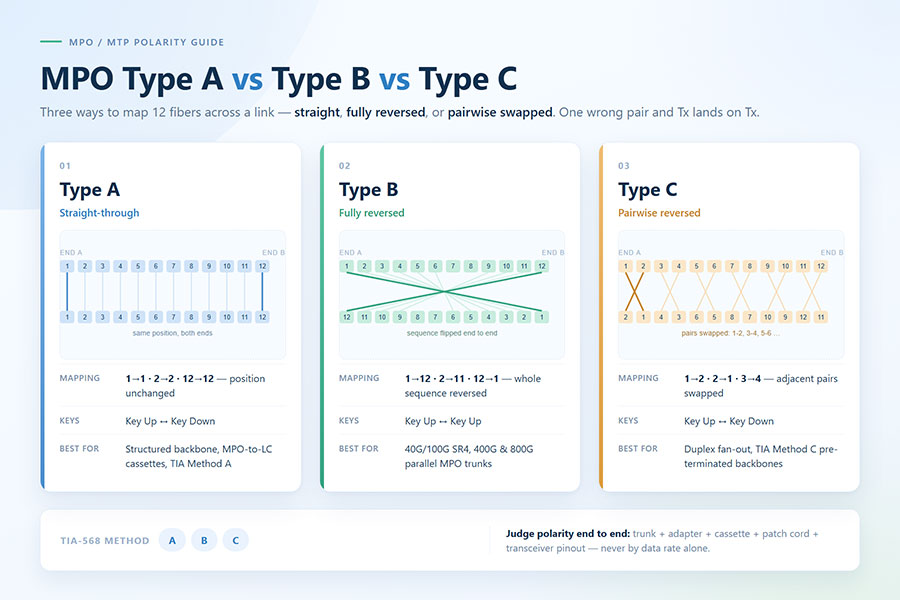
The optical interface also depends on the fiber type and connector design. Multimode and single-mode modules use different optical configurations, and connector choices such as LC and MPO are associated with different module architectures and lane arrangements.
7. Light Travels Through the Optical Fiber
Once coupled into the fiber, the modulated optical signal travels through the optical link. The fiber guides light through its core, allowing information to move between network devices without relying on an electrical signal traveling through a long copper conductor.
During transmission, the optical signal is affected by several physical factors:
Attenuation: Optical power decreases as light travels through the fiber and passes through connectors, splices and other components.
Dispersion: Different signal components may experience different propagation delays, spreading the received waveform over time.
Connector and splice loss: Imperfect connections introduce additional optical loss.
Reflections: Optical discontinuities can return a portion of the signal toward the source.
Environmental conditions: Temperature changes, mechanical stress and fiber routing can influence link performance.
The receiver must be able to distinguish the transmitted data after these effects have altered the optical signal. This is why optical power budget, receiver sensitivity, transmitter characteristics and fiber quality must be considered together during link planning.
8. The Photodetector Converts Light Back into Electrical Current
At the receiving end, the optical signal enters the receiver section of the transceiver. Optical coupling components direct the incoming light toward a photodetector, which converts optical energy into an electrical current.
Two commonly used photodetector types are PIN photodiodes and avalanche photodiodes (APDs).
| Feature | PIN Photodiode | APD |
|---|---|---|
| Detection principle | Converts incoming photons into photocurrent. | Uses internal avalanche multiplication to provide additional signal gain. |
| Internal gain | No avalanche multiplication. | Provides internal gain through a high electric field. |
| Bias requirements | Generally simpler bias requirements. | Requires controlled higher reverse-bias voltage. |
| Design considerations | Noise, sensitivity and bandwidth. | Gain, excess noise, bias stability and temperature behavior. |
The photodetector does not directly produce the same type of electrical signal that the host device originally transmitted. Its output is a relatively small photocurrent that must be amplified and processed by the receiver circuitry.
9. The TIA Amplifies the Weak Receiver Signal
The photodetector generates a current proportional to the received optical power. This current is often very small, so the receiver uses a transimpedance amplifier (TIA) to convert it into a usable voltage signal.
The TIA is a critical part of the optical receiver. It must provide sufficient gain while controlling noise and maintaining the bandwidth needed for the incoming data rate.
Additional receiver amplification and equalization may follow the TIA. These circuits help condition the signal for subsequent clock recovery, decoding or DSP processing. Their exact arrangement depends on the receiver architecture.
10. Clock Recovery and Data Reconstruction
After amplification and signal conditioning, the receiver must recover the transmitted information. High-speed digital communication requires the receiver to identify the correct sampling times as well as the signal values.
Clock and data recovery circuitry extracts timing information from the incoming waveform. The receiver uses this timing reference to sample the signal and determine the transmitted symbols. Depending on the module, this function may be implemented in a CDR circuit, DSP or host-side receiver architecture.
For PAM4 systems, the receiver distinguishes among four signal amplitude levels. Each symbol represents two bits, increasing the number of bits transmitted per symbol compared with NRZ. However, the smaller separation between PAM4 levels makes signal quality, noise control and equalization particularly important.
| Characteristic | NRZ | PAM4 |
|---|---|---|
| Signal levels | 2 | 4 |
| Bits per symbol | 1 | 2 |
| Signal interpretation | One binary decision between two levels. | One of four amplitude levels is identified. |
| Design considerations | Signal integrity and timing margins. | More demanding amplitude accuracy, noise control and equalization. |
Once the receiver has recovered the data, it delivers the reconstructed electrical signal through the module's host interface to the switch, router, server or network adapter.
11. How Multiple Lanes Work in High-Speed Transceivers
Modern optical transceivers achieve high aggregate data rates by operating multiple electrical and optical lanes in parallel. Instead of relying on one extremely high-speed channel, the module distributes data across several lanes and combines their capacity into a single network interface.
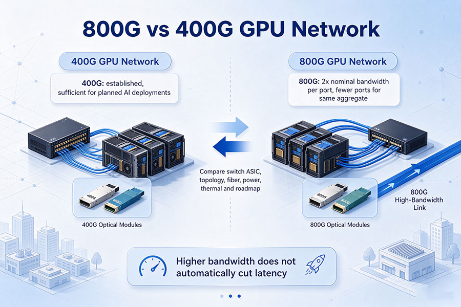
The lane configuration depends on the standard and product design. A 400G module, for example, may use multiple electrical lanes and corresponding optical channels. Some optical interfaces transmit over parallel fibers, while wavelength-multiplexed designs combine several optical channels onto fewer fibers.
| Module Data Rate | Typical Architecture Direction | Design Considerations |
|---|---|---|
| 100G | One or multiple electrical and optical lanes, depending on the interface. | NRZ or PAM4 implementations, fiber type and optical reach. |
| 400G | Multi-lane electrical and optical architecture. | Lane mapping, modulation, parallel or wavelength-multiplexed optics. |
| 800G | Higher-rate multi-lane architecture, commonly using 100G-class electrical signaling per lane. | Electrical channel performance, DSP design, thermal management and optical interface. |
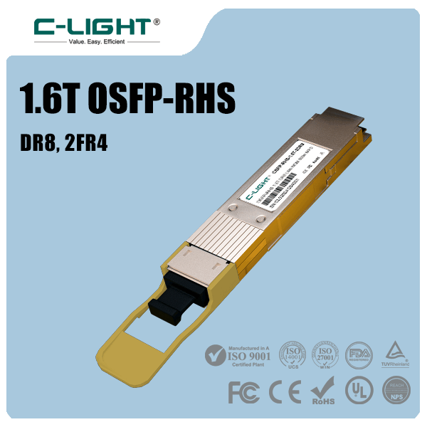
| 1.6T | Next-generation multi-lane architecture targeting higher per-lane signaling rates. | 224G-class electrical signaling, advanced packaging, power density and cooling. |
These are broad architectural directions rather than universal lane mappings. The actual number of lanes, signaling rate, modulation format and optical arrangement must be checked against the relevant Ethernet, InfiniBand or module specification.
12. The Control and Monitoring Circuits Keep the Module Operating
Data transmission is not the only activity inside an optical transceiver. A management controller and supporting circuits monitor operating conditions, manage module functions and communicate diagnostic information to the host system.
Depending on the module and management standard, monitored parameters may include:
Temperature: Reports the module's internal temperature for thermal monitoring.
Supply voltage: Tracks the electrical supply condition.
Transmit optical power: Monitors the transmitter's optical output.
Receive optical power: Reports the optical power detected by the receiver.
Laser bias current: Provides information about the transmitter's operating condition.
Module status and alarms: Indicates faults or operating conditions that require attention.
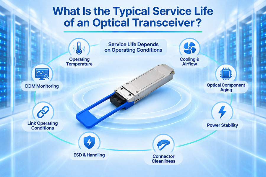
Digital diagnostics help network operators identify issues such as unexpected optical-power changes, overheating or abnormal operating conditions. The available monitoring functions depend on the module's hardware, firmware and management interface.
13. What Determines the Quality of Data Transmission?
A transceiver's ability to transmit and recover data depends on the complete electrical and optical link. A module can meet its nominal data rate while still experiencing errors if the host channel, fiber path, optical power or environmental conditions are outside the required limits.
| Parameter | What It Indicates | Why It Matters |
|---|---|---|
| Transmit Optical Power | Optical power launched by the transmitter. | Determines the available optical signal level at the beginning of the link. |
| Receiver Sensitivity | Minimum received optical power for specified performance. | Defines the receiver's ability to detect a weak signal. |
| Optical Power Budget | Difference between transmitter output and receiver sensitivity, subject to specified conditions. | Indicates the available allowance for fiber, connector and other link losses. |
| Extinction Ratio | Relationship between optical power levels representing different transmitted states. | Affects the quality and distinguishability of the transmitted signal. |
| BER | Bit error rate measured under defined test conditions. | Indicates how reliably the receiver reconstructs transmitted data. |
| Jitter | Variation in signal timing. | Can reduce sampling margin and increase the risk of data errors. |
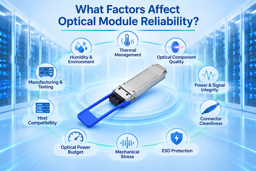
| Temperature | Thermal operating condition of the module. | Can affect laser characteristics, receiver performance and overall reliability. |
These parameters should be evaluated together. For example, adequate received optical power does not automatically guarantee a low bit error rate if the signal is distorted by dispersion, reflections, electrical noise or insufficient receiver margin.
14. A Practical Example: Data Transmission Through a 400G OSFP Module
A 400G OSFP transceiver illustrates how the different subsystems work together in a modern high-bandwidth network. When installed in a compatible switch or server interface, the module receives high-speed electrical data from the host, processes it according to its architecture and converts it into optical signals for fiber transmission.
At the receiving end, a compatible optical interface detects the incoming signal, converts it into electrical current and reconstructs the data for the host device. The module's optical interface, lane configuration, wavelength and reach must match the corresponding link requirements.
C-LIGHT's 400G OSFP product family is designed for AI data centers, cloud computing and high-performance computing networks. The listed configurations include SR4, DR4, FR4 and LR4 options, with different fiber types, connectors and transmission distances.
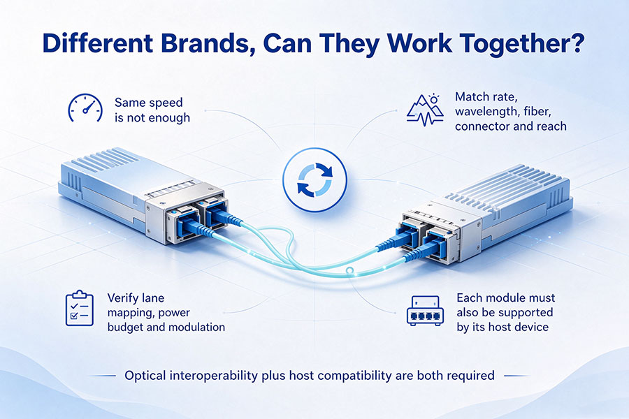
For a real deployment, engineers should verify the exact module part number, host compatibility, optical standard, fiber type, connector, transmission distance and operating temperature. The 400G label alone does not establish that two modules are interchangeable.
15. Why Transmitter and Receiver Design Must Be Evaluated Together
The transmitter and receiver form one optical communication system. Improving only one side does not guarantee better end-to-end performance. A high-output transmitter cannot overcome every receiver limitation, and a highly sensitive receiver cannot recover information that has been severely distorted before detection.
Successful optical link engineering therefore requires coordinated design across the host electrical interface, transmitter, fiber channel, receiver and network equipment. At higher data rates, lane mapping, signal integrity, DSP architecture, thermal performance and optical power margins become increasingly important.
16. Conclusion
Inside an optical transceiver, data passes through a carefully coordinated sequence of electrical and optical operations. The transmitter receives electrical signals, conditions them, drives a laser or modulator and launches the resulting optical signal into the fiber. The receiver detects the incoming light, converts it into photocurrent, amplifies and processes the signal, recovers timing and reconstructs the original data.
Every stage contributes to the reliability and performance of the optical link. As networks move toward 400G, 800G and 1.6T connectivity, the coordination of high-speed electrical interfaces, photonic components, signal processing and thermal design becomes increasingly important.
C-LIGHT provides optical transceiver solutions for data center, telecom, Ethernet and high-performance computing applications. For assistance with module selection, equipment compatibility or optical connectivity requirements, Contact C-LIGHT.
 >

 >
 >
 >
 >
 >
 >
 >