TEL:+86 132 6656 7067





Every optical receiver must convert incoming light into an electrical signal before the original data can be recovered. As data rates increase, this conversion stage becomes increasingly important: the detector must respond quickly to changing optical power while introducing as little noise and distortion as possible.
The PIN photodiode is one of the most widely used components for this task. Its semiconductor structure converts absorbed photons into electrical current, providing a direct interface between the optical fiber and the receiver's electronic circuitry. Combined with a low-noise transimpedance amplifier (TIA), it supports high-speed signal detection in data center transceivers, enterprise networks and telecommunications equipment.
1. What Is a PIN Photodiode?
A PIN photodiode is a semiconductor light detector consisting of three main regions: a positively doped P region, an intrinsic I region and a negatively doped N region. The intrinsic region is positioned between the P and N regions and provides the primary light-absorption area.
When photons enter the semiconductor and are absorbed, they generate electron-hole pairs. Under an applied reverse-bias electric field, these charge carriers move in opposite directions, producing a photocurrent proportional to the incident optical power within the detector's linear operating range.
The name PIN comes directly from its three-layer structure:
P region: Positively doped semiconductor layer.
I region: Intrinsic or lightly doped absorption region.
N region: Negatively doped semiconductor layer.
The intrinsic region helps increase the optical absorption volume while controlling junction capacitance and carrier transit characteristics. These properties make the PIN structure suitable for optical detection at high data rates.
2. How Does a PIN Photodiode Convert Light into Electrical Current?
The operating process is based on the photoelectric effect in a semiconductor. When incoming optical energy is absorbed, electrons gain enough energy to move into the conduction band, leaving holes in the valence band.
The reverse-bias electric field separates these electron-hole pairs. Electrons move toward the N-side contact, while holes move toward the P-side contact. Their movement creates an electrical current that follows changes in the received optical power.
The conversion process can be divided into four stages:
Photon absorption: Incoming light enters the photodiode's active region.
Carrier generation: Absorbed photons generate electron-hole pairs.
Carrier separation: The electric field drives electrons and holes toward opposite contacts.
Photocurrent generation: The resulting current carries information about the received optical signal.
3. The Relationship Between Optical Power and Photocurrent
One of the most important PIN photodiode characteristics is responsivity, which describes how much electrical current is generated for a given amount of incident optical power.
Where:
Iph: Photocurrent generated by the detector, measured in amperes.
R: Photodiode responsivity, measured in amperes per watt (A/W).
Popt: Incident optical power, measured in watts.
For example, if a photodiode has a responsivity of 0.8 A/W and receives 100 μW of optical power, its idealized photocurrent is:
This relationship is useful for understanding receiver operation and estimating the electrical signal available to the TIA. Actual receiver performance also depends on dark current, noise, bandwidth, optical coupling and the amplifier characteristics.
4. What Happens Inside the Optical Receiver?
The PIN photodiode is only one part of the receiver. After optical detection, the generated photocurrent is generally too small to drive the host interface directly. It must first be converted into a usable voltage signal and processed by the receiver electronics.
A simplified direct-detection receiver signal path is:
↓
Optical coupling and filtering
↓
PIN photodiode
↓
Transimpedance amplifier (TIA)
↓
Receiver amplifier and equalization
↓
CDR / DSP, where applicable
↓
Host electrical interface
The main stages have different responsibilities:
| Receiver Component | Main Function | Impact on Performance |
|---|---|---|
| Optical coupling structure | Directs incoming light onto the detector | Affects optical coupling efficiency and received power |
| PIN photodiode | Converts photons into photocurrent | Determines responsivity, detection bandwidth and detector noise |
| TIA | Converts photocurrent into voltage | Influences receiver sensitivity, noise and electrical bandwidth |
| Receiver amplifier | Provides additional signal amplification and conditioning | Helps establish suitable signal amplitude and dynamic range |
| CDR or DSP | Performs timing recovery or digital signal processing where implemented | Supports reliable data recovery at the required lane rate |
The exact architecture varies by transceiver. Some receivers integrate the photodiode and TIA into a ROSA, while others use different levels of photonic and electronic integration. Not every module contains a separate CDR or DSP stage.
5. Why Is the TIA Important to PIN Photodiode Performance?
A PIN photodiode produces a relatively small current, particularly when the received optical power is low. The TIA converts this current into a voltage signal that subsequent receiver circuits can process.
The TIA is therefore closely connected to the practical sensitivity of a PIN-based receiver. Even if the photodiode has good responsivity, excessive amplifier noise or insufficient bandwidth can prevent the receiver from recovering weak or rapidly changing signals reliably.
Important TIA design considerations include:
Transimpedance gain: Determines the voltage generated for a given input current.
Input-referred noise: Affects the minimum detectable optical signal.
Bandwidth: Determines how quickly the receiver can respond to signal transitions.
Dynamic range: Defines the range of input currents that can be handled without unacceptable distortion.
Stability: Helps prevent unwanted oscillation and signal degradation.
Photodiode capacitance and TIA input characteristics must also be considered together. Excessive input capacitance can restrict bandwidth and affect noise performance, making detector and amplifier co-design important in high-speed receivers.
6. Key PIN Photodiode Performance Parameters
The performance of a PIN photodiode is determined by several optical and electrical characteristics. These parameters influence the receiver's ability to detect weak signals and follow high-speed data transitions.
| Parameter | Definition | Why It Matters |
|---|---|---|
| Responsivity | Photocurrent generated per unit of incident optical power | Determines the detector's optical-to-electrical conversion efficiency |
| Dark current | Current flowing without incident optical illumination | Contributes to detector noise and affects weak-signal measurements |
| Junction capacitance | Electrical capacitance associated with the photodiode junction | Influences receiver bandwidth and electrical matching |
| Bandwidth | Frequency range over which the detector responds effectively | Determines suitability for high-speed optical signals |
| Quantum efficiency | Efficiency of converting incident photons into collected charge carriers | Influences responsivity |
| Linearity | How consistently photocurrent follows incident optical power | Helps preserve signal-level accuracy |
| Saturation level | Input level beyond which the detector or receiver response becomes nonlinear | Defines the upper end of the usable optical input range |
These parameters should be evaluated under the intended wavelength, bias voltage, temperature and operating conditions. A detector with high responsivity is not necessarily the best choice if its capacitance, noise or bandwidth is unsuitable for the target data rate.
7. How Wavelength Affects PIN Photodiode Selection
Photodiode materials have different absorption characteristics, so the semiconductor material must match the wavelength of the incoming optical signal.
Silicon photodiodes are commonly used for shorter wavelengths, including the 850nm region used by many multimode data center links. InGaAs photodiodes are widely used for 1310nm and 1550nm single-mode optical communication because their absorption characteristics are suitable for these wavelength bands.
| Wavelength Region | Common Detector Material | Typical Application |
|---|---|---|
| 850nm | Silicon (Si) | Short-reach multimode fiber and VCSEL-based transceivers |
| 1310nm | InGaAs | Single-mode data center links and access networks |
| 1550nm | InGaAs | Longer-reach single-mode and DWDM systems |
Material selection is only one part of detector design. Responsivity, absorption-layer thickness, capacitance, packaging and receiver bandwidth must also meet the requirements of the optical interface.
8. PIN Photodiode vs. APD: What Is the Difference?
PIN photodiodes and avalanche photodiodes (APDs) are both used to detect optical signals, but they use different mechanisms to generate the receiver current.
A PIN photodiode produces photocurrent directly from the generated electron-hole pairs. An APD applies a much stronger electric field in its multiplication region, causing impact ionization and internal carrier multiplication. This provides additional current gain before the signal reaches the amplifier.
| Characteristic | PIN Photodiode | APD |
|---|---|---|
| Detection mechanism | Direct photocarrier generation | Photocarrier generation with avalanche multiplication |
| Internal gain | No avalanche gain | Provides internal multiplication gain |
| Receiver noise | No avalanche multiplication noise | Additional excess noise from multiplication |
| Bias requirements | Generally lower and simpler | Higher reverse bias with tighter control |
| Receiver complexity | Relatively simple | More complex bias and temperature management |
| Typical application direction | Short-reach and many high-speed data links | Links requiring additional sensitivity under constrained power budgets |
APDs can improve receiver sensitivity when optical input power is limited, but their internal gain also introduces excess noise and additional bias requirements. PIN photodiodes offer a simpler, more linear detection mechanism and can provide excellent performance when paired with a sufficiently low-noise TIA.
Neither detector type is universally superior. Selection depends on the link budget, data rate, receiver noise, power consumption, operating temperature and cost requirements.
9. Why PIN Photodiodes Are Widely Used in High-Speed Transceivers
Modern data center optical links require receiver components that can detect high-speed optical signals without adding excessive noise or limiting the available bandwidth. PIN photodiodes are well suited to many of these applications because their structure supports fast carrier collection and relatively straightforward receiver integration.
Their main advantages include:
High-speed response: Properly designed PIN photodiodes can support high-bandwidth optical detection.
Low detector noise: They avoid the excess multiplication noise associated with APDs.
Simple biasing: Their operating requirements are generally less demanding than avalanche detectors.
Good linearity: Photocurrent can track optical input power over the specified operating range.
Integration potential: PIN detector arrays can be integrated into multi-lane receiver architectures.
In PAM4 systems, the receiver must distinguish four optical amplitude levels. The photodiode itself does not decode these levels; it converts them into corresponding current levels. The TIA and subsequent signal-processing circuits must preserve sufficient amplitude separation and timing information for reliable decisions.
10. PIN Photodiode Arrays in 400G and 800G Optical Modules
High-speed optical transceivers often use multiple optical lanes to achieve their aggregate data rates. Instead of relying on one photodetector, a parallel optical receiver can integrate several PIN photodiodes into an array, with each detector handling a separate optical lane.
For example, an 800G SR8 transceiver can use eight 100G PAM4 receive lanes. Each lane has its own optical detection path, allowing the module to recover multiple data streams in parallel.
| Optical Architecture | Receive Lane Structure | Typical Receiver Technology |
|---|---|---|
| 100G SR4 | 4 optical receive lanes | PIN photodetector array |
| 400G SR8 | 8 optical receive lanes | PIN photodetector array |
| 800G SR8 | 8 optical receive lanes | High-speed PIN photodetector array |
| 800G DR4 | 4 optical receive lanes | PIN photodetectors in a single-mode receiver architecture |
The detector material and optical coupling design depend on the wavelength and fiber interface. For example, 850nm VCSEL-based SR links commonly use silicon photodetectors, while 1310nm single-mode links commonly use InGaAs detectors.
11. Common PIN Photodiode Receiver Problems
Although PIN photodiodes are reliable receiver components, several conditions can reduce detection performance or cause link instability.
Insufficient optical input: Low received power produces a smaller photocurrent, making the signal more vulnerable to TIA and receiver noise.
Excessive optical input: Very high received power can push the photodiode or receiver amplifier outside its linear operating range, causing distortion or overload.
High dark current: Increased dark current can contribute to noise and may indicate a device or environmental issue, depending on the operating conditions.
Excessive capacitance: Detector capacitance and parasitic electrical effects can limit bandwidth and degrade high-speed response.
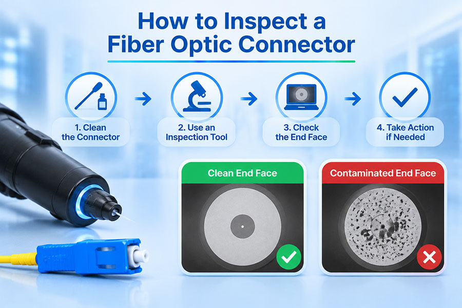
Optical coupling loss: Poor alignment, contamination or connector loss reduces the optical power reaching the detector.
Thermal variation: Temperature can affect detector characteristics and receiver electronics, changing the overall operating margin.
Diagnosing these issues requires measurements across the complete receiver path. A low photocurrent reading does not automatically mean the photodiode is defective; the optical input power, coupling path, wavelength and receiver electronics must also be checked.
12. How PIN Photodiode Receivers Are Tested
Receiver testing verifies whether the photodiode and associated electronics can recover optical signals within the required operating range. Component-level tests focus on detector characteristics, while transceiver-level tests evaluate complete link performance.
| Test Item | What Is Measured | Purpose |
|---|---|---|
| Responsivity | Photocurrent relative to incident optical power | Verifies optical-to-electrical conversion efficiency |
| Dark current | Current without optical input | Evaluates detector leakage and baseline current |
| Bandwidth | Frequency response of the detector | Checks suitability for the target signal rate |
| Receiver sensitivity | Minimum optical input for a specified BER under defined conditions | Evaluates weak-signal detection performance |
| Overload performance | Receiver behavior at high optical input levels | Checks the upper operating limit |
| BER testing | Bit errors under specified optical and electrical conditions | Verifies end-to-end receiver performance |
| Temperature testing | Receiver performance across rated temperatures | Checks operating stability |
For high-speed PAM4 interfaces, receiver testing must follow the applicable interface specification and test methodology. Sensitivity measurements should state the relevant BER target, FEC condition, signal format and stressed-input conditions because these factors affect the reported result.
13. PIN Photodiodes in C-LIGHT High-Speed Optical Transceivers
PIN photodetectors are important components in many high-speed optical receiver architectures. Their role becomes particularly visible in parallel optical modules, where multiple detector channels recover independent optical lanes.
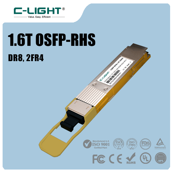
C-LIGHT's 800G OSFP Optical Transceiver portfolio includes SR8 configurations for short-reach multimode links as well as single-mode options such as DR8 and 2×FR4. The SR8 implementation uses an 850nm VCSEL transmitter array and a PIN photodetector array to support eight optical lanes.
For a single-mode example, C-LIGHT's 800G 1DR4 500m OSFP-RHS uses EML transmitters and PIN photodetectors for its 1310nm optical lanes. This illustrates that PIN receivers are not limited to 850nm multimode systems; the detector material and design are selected according to the operating wavelength and receiver requirements.
When selecting a high-speed optical transceiver, engineers should evaluate receiver sensitivity, overload limits, wavelength, fiber type, optical power budget, lane configuration and host compatibility together. C-LIGHT provides optical connectivity solutions for data center, Ethernet and high-performance computing applications. For product specifications or application support, Contact C-LIGHT.
14. Conclusion
The PIN photodiode is a fundamental component in optical receivers because it converts incoming photons into electrical current through semiconductor photodetection. Its P-I-N structure supports efficient carrier collection, low detector noise, good linearity and high-speed operation.
Working together with a TIA and receiver signal-processing circuits, PIN photodiodes enable optical transceivers to recover data across multimode and single-mode fiber links. Their use in multi-lane 400G and 800G modules also demonstrates how this established detector technology continues to support increasingly demanding data center interconnects.
Ultimately, receiver performance depends on the complete detection chain. Photodiode responsivity, dark current, capacitance and bandwidth must be matched with amplifier noise, optical input power and the target transmission interface to achieve reliable high-speed communication.
 >

 >
 >
 >
 >
 >
 >
 >