TEL:+86 132 6656 7067





A pluggable optical module contains several electrical interfaces that connect the host networking device with the module's internal optical and electronic components. These connections do much more than carry data. They also supply power, provide management access, control module operating states and support monitoring.
The main electrical interfaces can be divided into two groups: the external host-to-module interface and the internal electrical connections between functional components. The external interface includes high-speed differential lanes, low-speed management signals, control pins, power contacts and ground connections. Inside the module, additional electrical paths connect the DSP or CDR, laser driver, receiver amplifier, microcontroller and power-management circuits.
Understanding these interfaces is important when evaluating module compatibility, signal integrity, power consumption, initialization and high-speed data transmission.
1. Overview of Electrical Interfaces in a Pluggable Optical Module
A pluggable optical module connects to a switch, router, server or other host through a standardized electrical connector. The host provides high-speed electrical signals and power, while the module handles optical transmission, reception and management functions.
The main electrical interface categories include:
High-speed data interface: Differential electrical lanes carrying transmit and receive data between the host and module.
Management interface: A low-speed communication channel used for identification, configuration and diagnostics.
Control and status signals: Discrete signals for module presence, reset, low-power operation and interrupt reporting.
Power interface: Electrical contacts supplying the module's operating voltage and current.
Ground interface: Return paths and reference connections for power and high-speed signaling.
Optional timing and auxiliary interfaces: Reference clock or other signals used by particular module designs.
↓
High-Speed Electrical Lanes + Management + Control + Power
↓
Pluggable Optical Module
↓
DSP / CDR / Laser Driver / TIA / Optical Components
↓
Optical Fiber
Not every module uses every optional interface. The exact pin assignment, electrical characteristics and management implementation depend on its form factor and applicable Multi-Source Agreement (MSA) or industry specification.
2. High-Speed Differential Data Interfaces
The high-speed electrical interface is the primary data connection between the host device and the optical module. It carries the electrical signals that are converted into optical signals for transmission and carries recovered electrical data back to the host.
These signals are generally transmitted through differential pairs. Each pair carries complementary electrical signals, allowing the receiver to detect the voltage difference between the two conductors rather than relying on a single-ended voltage referenced to ground.
Differential signaling offers several advantages:
Better rejection of common-mode noise.
Improved signal integrity at high data rates.
Reduced electromagnetic interference when properly implemented.
Support for high-speed serial communication over compact electrical connections.
The high-speed interface has two directional paths:
| Signal Direction | Electrical Path | Module Function |
|---|---|---|
| Host-to-module | Host Tx differential lanes → Module Rx electrical interface | Receives electrical data from the host for optical transmission |
| Module-to-host | Module Tx electrical interface → Host Rx differential lanes | Returns recovered electrical data to the host |
The Tx and Rx labels are always relative to the device being described. A host transmitter connects to the module's receive-side electrical input, while the module's electrical output connects to the host receiver.
The number of lanes depends on the module generation and application. A four-lane 100G QSFP28 interface, for example, uses four electrical transmit lanes and four electrical receive lanes. Many 400G QSFP-DD and OSFP implementations use eight lanes in each direction, although the supported lane rates and electrical architecture depend on the particular interface standard.
3. SerDes Interface and Electrical Lane Mapping
SerDes stands for Serializer/Deserializer. It converts parallel data inside the host ASIC into high-speed serial electrical signals and performs the reverse operation on received data.
The host SerDes communicates with the module through the electrical host interface. Depending on the module architecture, the module may perform additional signal conditioning, clock recovery, retiming or digital signal processing before converting the electrical data into optical signals.
Lane mapping determines how electrical channels correspond to the module's internal processing channels and optical media lanes.
| Module Example | Typical Host Electrical Lane Structure | Aggregate Data Rate |
|---|---|---|
| 100G QSFP28 | 4 × 25G-class lanes | 100G |
| 200G QSFP56 | 4 × 50G-class lanes | 200G |
| 400G QSFP-DD / OSFP | 8 × 50G-class PAM4 lanes in common implementations | 400G |
| 800G QSFP-DD / OSFP | 8 × 100G-class PAM4 lanes in common implementations | 800G |
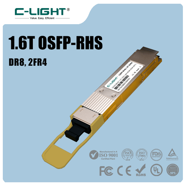
| 1.6T OSFP | 8 × 200G-class PAM4 lanes in representative architectures | 1.6T |
These are representative electrical lane arrangements, not universal pin-level definitions. Actual signaling rates, encoding, modulation, lane allocation and host interface requirements must be checked against the relevant MSA and product specification.
For a module with DSP-based signal processing, the electrical interface may connect to a DSP that performs equalization, clock recovery and other signal-conditioning functions. In a linear or lower-power architecture, some of these functions may instead be handled by the host SerDes and simpler module circuitry.
4. I2C and the Low-Speed Management Interface
High-speed differential lanes carry the network traffic, but the host also needs a separate way to identify and manage the module. This is the role of the low-speed management interface.
Many pluggable optical modules use a two-wire management interface based on I2C or a compatible two-wire interface. It allows the host to communicate with the module's management controller and access standardized registers or memory maps.
The management interface is used for tasks such as:
Reading module identification and vendor information.
Retrieving supported data rates and application capabilities.
Configuring supported operating modes.
Reading temperature, voltage and optical diagnostic information.
Checking warning and alarm conditions.
Accessing module status and data-path information.
The management bus is a low-speed control channel, not the main user-data path. A module can respond to management requests even when its optical data link has not yet been established.
Successful I2C communication confirms that the host can access the module's management interface. It does not prove that the high-speed electrical lanes, optical transmitter, receiver or remote fiber link are functioning correctly.
5. CMIS and Form-Factor Management Protocols
The physical management connection and the management protocol are related but different concepts. The electrical connection defines how signals travel between the host and module, while the management protocol defines how information is organized and exchanged.
Older and newer module families use different management specifications. SFP modules commonly use SFF-8472, while QSFP-family modules have used SFF-8636 and related specifications. Modern QSFP-DD and OSFP modules commonly use the Common Management Interface Specification (CMIS).
| Module Family | Common Management Specification | Management Functions |
|---|---|---|
| SFP / SFP+ | SFF-8472 | Identification, digital diagnostics and control |
| QSFP / QSFP28 | SFF-8636 | Module monitoring, control and lane-related information |
| QSFP-DD | CMIS | Application selection, data-path configuration and monitoring |
| OSFP | CMIS | Module management, application configuration and diagnostics |
CMIS provides a common framework for managing increasingly complex pluggable modules. It defines module states, application descriptors, data-path management and monitoring structures. This is particularly important for modules with multiple high-speed lanes and configurable operating modes.
For example, the host may use CMIS to identify supported applications, select an appropriate configuration and activate the required data paths. The module then reports its operating state through the management interface.
6. Module Control and Status Signals
In addition to the two-wire management bus, pluggable modules may have dedicated low-speed control and status pins. These signals allow the host to perform basic operations without relying entirely on register transactions.
Common signals include:
| Signal | Typical Function | Operational Role |
|---|---|---|
| ModPrsL | Module present indication | Allows the host to detect whether a module is inserted |
| ResetL | Module reset control | Requests a hardware reset where supported |
| LPMode | Low-power mode control | Requests or indicates a low-power operating condition |
| IntL | Interrupt indication | Alerts the host to a module event or status change |
| ModSelL | Module selection | Used in applicable form factors to select a module for management access |
Signal names, polarity, availability and behavior vary by form factor and specification revision. Some functions are handled through management registers rather than separate pins in particular implementations.
These signals are especially important during module insertion, reset, initialization and fault reporting. For example, module presence detection allows the host to recognize insertion before it attempts to read the module's identification information.
7. Power Supply and Ground Interfaces
Optical modules require electrical power for their internal circuits. Power contacts on the module connector supply the voltage rails used by the DSP, laser driver, receiver circuitry, management controller and other components.
Different module generations have different power requirements. Higher-speed modules often contain more complex signal-processing circuits and optical components, increasing the importance of power delivery and thermal design.
The power interface must support:
Stable supply voltage within the specified operating range.
Sufficient current capacity for the module's operating mode.
Controlled power-up and power-down sequencing.
Appropriate decoupling and noise management.
Reliable ground connections and return paths.
Ground contacts have several roles. They provide return paths for power, establish electrical references and support the controlled return-current paths needed by high-speed differential signaling.
In high-speed designs, connector layout and PCB grounding are critical. Poor return-path continuity, impedance discontinuities or inadequate power decoupling can introduce noise and degrade signal integrity.
A form-factor specification may define the power levels a module and host interface must support. Actual operating power depends on the module design, data rate, optical reach, DSP architecture and operating conditions.
8. Reference Clock and Auxiliary Electrical Interfaces
Some pluggable optical modules use additional timing or auxiliary signals. These may include reference clocks or other application-specific electrical connections.
A reference clock can provide a timing source for circuits that need to synchronize their operation. Its role depends on the module architecture and the host interface requirements.
However, a separate reference clock is not mandatory for every pluggable optical module. Many modules recover timing from the incoming serial data stream through clock and data recovery (CDR) circuits, or rely on the host's SerDes clocking architecture.
Other auxiliary connections may support specific applications or form-factor features. Their presence and function must be verified against the applicable connector and module specification.
9. Internal Electrical Connections Between Module Components
The host connector is only the external entry point. Inside the module, electrical connections distribute data, power and control signals among several functional components.
A typical DSP-based module may include a microcontroller, power-management IC, DSP or CDR, laser driver, transmitter optical assembly, receiver optical assembly and supporting circuits.
Host Electrical Input
↓
DSP / Signal Conditioning / CDR (where used)
↓
Laser Driver
↓
Laser or Optical Modulator
↓
Optical Fiber
Receive Direction
Optical Fiber
↓
Photodetector
↓
TIA / Receiver Amplifier
↓
DSP / Equalization / CDR (where used)
↓
Host Electrical Output
The internal electrical connections serve different purposes:
| Internal Component | Electrical Connection | Main Function |
|---|---|---|
| DSP | High-speed differential data, clock and power connections | Signal processing, equalization and other supported functions |
| CDR | High-speed data and timing connections | Recovers clock timing from serial data where implemented |
| Laser driver | Data input, bias control, modulation control and power | Drives the laser or modulator in the transmit path |
| TIA | Photodetector input and amplified electrical output | Converts photodiode current into a usable voltage signal |
| Microcontroller | Management bus, control lines and power | Manages module configuration, monitoring and status |
| PMIC | Input power and regulated output rails | Distributes suitable power to internal circuits |
| Monitor photodiode circuit | Monitor current and control feedback | Supports transmitter optical-power monitoring and control |
The exact arrangement varies. Some modules integrate several functions into a single IC, while others use separate components. Linear optical modules may omit a conventional DSP retimer, and some architectures use external or shared timing resources.
10. Electrical Interface Differences Between SFP, QSFP-DD and OSFP
Different module form factors use different connector layouts, lane counts, mechanical dimensions and power arrangements. These differences affect the electrical interface between the module and host.
| Form Factor | Typical High-Speed Lane Structure | Management Approach | Common Applications |
|---|---|---|---|
| SFP / SFP+ | One Tx and one Rx lane | SFF-8472 in common implementations | 1G, 10G and related single-lane applications |
| QSFP28 | Four Tx and four Rx lanes | SFF-8636 | 40G and 100G connectivity |
| QSFP-DD | Eight Tx and eight Rx lanes | CMIS in common implementations | 200G, 400G and 800G modules |
| OSFP | Eight Tx and eight Rx lanes in common implementations | CMIS in common implementations | 400G, 800G and 1.6T platforms |
The table describes common lane arrangements rather than every possible implementation. Electrical signaling rates and application support vary with module generation and host platform.
QSFP-DD and OSFP are both designed to support high-density, high-bandwidth applications, but they have different mechanical and electrical specifications. Their modules and cages should not be treated as interchangeable simply because they may support similar aggregate data rates.
11. How Electrical Interfaces Affect Signal Integrity
At high data rates, the electrical connection between the host and module becomes a critical part of the complete communication channel. The signal must travel through the host PCB, connector contacts, module PCB and internal signal-processing circuitry before reaching the optical transmitter or host receiver.
Several electrical factors influence signal integrity:
Insertion loss: Reduces signal amplitude as the signal travels through the electrical channel.
Return loss: Indicates reflections caused by impedance discontinuities.
Crosstalk: Allows unwanted energy from neighboring channels to interfere with the target signal.
Jitter: Changes the timing of signal transitions and reduces sampling margin.
Impedance continuity: Helps maintain predictable signal propagation through the connector and PCB.
Power integrity: Prevents supply noise from disturbing sensitive analog and high-speed circuits.
These issues become more challenging as electrical lane rates increase. PAM4-based interfaces, widely used in 400G and 800G modules, have smaller voltage separation between adjacent symbol levels than NRZ signaling at a comparable signal amplitude. This places tighter demands on the electrical channel and signal-processing design.
Host PCB layout, connector design, module PCB routing, equalization and thermal management must therefore be considered together.
12. What Happens When an Electrical Interface Fails?
A problem in one electrical interface can affect a different part of module operation. Identifying the affected interface helps narrow down the cause of a failure.
| Possible Interface Problem | Typical Symptom | Area to Investigate |
|---|---|---|
| High-speed Tx lane issue | Host data does not reach the module correctly | Host SerDes, connector, PCB channel and module input |
| High-speed Rx lane issue | Host cannot recover data from the module | Module output, connector and host receiver |
| Management bus failure | Module information or diagnostics cannot be read | I2C wiring, address, controller and host management logic |
| Control signal problem | Module cannot reset, enter the expected power mode or report status correctly | Control-pin connection and host control logic |
| Power supply issue | Module fails to initialize or behaves intermittently | Supply voltage, current capacity, sequencing and grounding |
| Internal component connection fault | Management may work while one data direction fails | DSP, CDR, laser driver, TIA and internal signal paths |
It is important to distinguish a management communication problem from a high-speed data-path problem. A module may be detectable and readable through I2C while its optical link remains down because of an electrical lane, transmitter, receiver or fiber issue.
13. C-LIGHT 400G OSFP and High-Speed Electrical Interfaces
High-speed optical modules require carefully coordinated electrical and optical interfaces. The host electrical lane structure must match the module's supported application, while the internal signal-processing architecture must support the required data rate and optical modulation format.
The C-LIGHT 400G OSFP Optical Transceiver is designed for AI data centers, cloud networks and high-performance computing applications.
The product information specifies an OSFP package, CMIS Rev. 5.2 management interface protocol and support for 400G optical configurations. Its electrical architecture uses eight high-speed channels, with representative signaling arrangements including 8 × 50G PAM4. Actual lane mapping depends on the selected module configuration and host application.
The product family includes SR4, DR4, FR4 and LR4 optical options, covering different fiber types and transmission distances. This allows the same general form-factor family to serve different data center connectivity requirements.
When integrating a 400G OSFP module, engineers should verify the host's electrical lane rate, modulation support, lane mapping, CMIS implementation, power capability, cooling conditions and optical application. Matching the physical form factor alone does not guarantee complete electrical or protocol compatibility.
14. Conclusion
The electrical interfaces inside a pluggable optical module perform several distinct functions. High-speed differential lanes carry transmit and receive data, while the I2C-based management interface provides module identification, configuration and diagnostics. Dedicated control signals support module operation, and power and ground contacts supply the electrical energy and reference paths required by internal circuits.
Inside the module, additional electrical connections link the DSP or CDR, laser driver, TIA, microcontroller and power-management components. Their arrangement depends on the module architecture and performance requirements.
As optical modules advance from 100G to 400G, 800G and 1.6T, the electrical interface becomes increasingly important to signal integrity, power delivery, thermal design and host compatibility. Understanding the complete electrical path—from host SerDes to internal optical components—is essential for reliable high-speed optical connectivity.
C-LIGHT provides optical transceiver solutions for Ethernet, InfiniBand, AI data centers and telecom networks. For help selecting a module based on form factor, electrical interface, data rate and host compatibility, Contact C-LIGHT.
 >

 >
 >
 >
 >
 >
 >
 >