TEL:+86 132 6656 7067





An optical module relies on two coordinated circuit systems to move information across a fiber link. The transmitter circuit accepts high-speed electrical data and controls the optical source, while the receiver circuit detects incoming light and reconstructs the electrical signal. Their performance depends on more than the laser and photodiode: drivers, amplifiers, timing circuits, bias controls and signal-processing devices all contribute to the operation of the module.
Although transmitter and receiver circuits perform opposite conversions, they share several engineering requirements. Both must maintain signal integrity, control noise, operate within defined electrical and thermal limits, and work with the host equipment's high-speed interface. Their detailed implementations vary with the module's data rate, optical reach, modulation format and form factor.
1. The Basic Circuit Architecture of an Optical Module
An optical transceiver contains a transmit path and a receive path. The transmit path converts electrical data into modulated light. The receive path converts incoming light into an electrical signal that the host device can process.
The diagram represents a typical functional arrangement, not a fixed circuit schematic. Some modules integrate several functions into one device, while others use separate driver, amplifier, CDR or DSP components. Linear optical modules may also omit conventional retiming and rely more heavily on the host SerDes.
2. How the Transmitter Circuit Processes Electrical Data
The transmitter begins at the module's electrical interface. A switch ASIC, network processor or server adapter sends differential high-speed signals through the host connector. These signals carry the data that must be converted into optical form.
Before driving the optical source, the transmitter circuitry may perform several operations:
Input termination: Provides the required electrical loading and helps maintain signal integrity at the interface.
Equalization: Compensates for frequency-dependent loss and waveform distortion in the electrical channel.
Clock and data recovery: Extracts timing information and, where implemented, regenerates the data stream.
DSP processing: Performs digital signal operations required by the module's transmission architecture.
Lane handling: Processes the electrical channels used to achieve the module's aggregate data rate.
These functions prepare the signal for optical modulation. Their exact location can vary: some processing is performed inside the optical module, while other functions remain in the host ASIC or SerDes.
3. The Laser Driver Circuit Controls the Optical Source
The laser driver is one of the most important transmitter components. It receives the electrical data signal and provides the controlled current or voltage drive required by the optical source or modulator.
For a directly modulated laser, the driver controls the laser current to create data-dependent changes in optical output power. For an externally modulated transmitter, the laser may provide continuous-wave light while a separate modulator changes the optical signal according to the electrical data.
A typical laser driver manages several operating parameters:
| Driver Function | Purpose | Engineering Consideration |
|---|---|---|
| Bias Current Control | Maintains the operating point of the laser. | Must remain within the source's specified operating range. |
| Modulation Current | Controls data-dependent changes in the optical output. | Affects optical modulation amplitude and signal quality. |
| Output Control | Adjusts drive conditions according to the transmitter design. | Must account for laser characteristics and temperature. |
| Fault Protection | Helps protect the laser and associated circuitry. | May include current limits and safety-related control functions. |
The driver must also deliver sufficiently fast transitions without introducing excessive noise or distortion. At higher data rates, parasitic capacitance, package inductance, impedance discontinuities and PCB layout become increasingly important.
4. Laser Bias and Automatic Power Control
Laser characteristics can change with temperature, operating conditions and component aging. A transmitter therefore needs a stable operating point to maintain the intended optical output.
Many designs use monitoring circuitry to measure laser-related parameters and adjust the bias conditions. A monitor photodiode, where included, can provide feedback about the emitted optical power. The control circuit compares the monitored value with a target and adjusts the laser drive conditions accordingly.
This feedback arrangement is commonly associated with automatic power control (APC). Its purpose is to maintain the required transmitter output within the module's specified operating range.
5. Optical Sources and Modulator Circuits
The transmitter's optical source depends on the module's wavelength, fiber type, reach and data-rate requirements. Different semiconductor devices require different drive and modulation arrangements.
| Optical Technology | Typical Use | Transmitter Circuit Requirement |
|---|---|---|
| VCSEL | Short-reach multimode optical links. | Laser driver controls the VCSEL operating current and data modulation. |
| DFB Laser | Single-mode optical transmission. | Requires controlled laser bias and modulation appropriate to the device architecture. |
| EML | High-performance single-mode links. | Uses a laser section and an electro-absorption modulator, with suitable drive and bias circuits. |
| External MZM | Selected high-speed and coherent optical systems. | Requires a modulator driver and bias-control circuitry for the Mach-Zehnder modulator. |
The laser or modulator converts the electrical drive into an optical waveform. Optical coupling components then direct the light toward the fiber interface. The transmitter's electrical and optical designs must be matched so that the output meets the required wavelength, power, modulation and signal-quality specifications.
6. How the Receiver Circuit Detects Incoming Light
The receiver circuit begins at the optical interface. Incoming light passes through the module's optical coupling system and reaches a photodetector. The photodetector converts the received optical energy into a small electrical current.
PIN photodiodes and avalanche photodiodes (APDs) are two common detector technologies. A PIN photodiode converts light into photocurrent without avalanche multiplication. An APD provides internal gain through an avalanche process, but requires more demanding bias and control arrangements.
| Feature | PIN Photodiode | APD |
|---|---|---|
| Signal conversion | Optical input becomes photocurrent. | Optical input becomes photocurrent with internal avalanche multiplication. |
| Internal gain | No avalanche gain. | Provides internal gain. |
| Bias control | Generally simpler. | Requires controlled reverse-bias voltage. |
| Design priorities | Responsivity, bandwidth and noise. | Gain, excess noise, bias stability and temperature behavior. |
The photodetector's output is not yet a suitable high-speed digital signal. Its photocurrent must be amplified and conditioned before the receiver can reliably identify the transmitted data.
7. The Transimpedance Amplifier Converts Current into Voltage
The transimpedance amplifier (TIA) is the first major electronic amplification stage in many optical receivers. It converts the photodetector's small output current into a voltage signal that subsequent receiver circuits can process.
Receiver sensitivity depends heavily on the combined performance of the photodetector and TIA. The TIA must provide enough gain to detect weak signals while keeping input-referred noise low and maintaining sufficient bandwidth.
Its design involves several competing requirements:
Gain: Converts small photocurrents into a measurable voltage signal.
Bandwidth: Supports the required data rate and signal spectrum.
Noise: Limits unwanted electrical fluctuations that can obscure the received signal.
Dynamic range: Handles the expected range of optical input power without unacceptable distortion or saturation.
Stability: Maintains predictable operation across specified temperature and supply conditions.
Increasing TIA gain without considering bandwidth and noise can reduce overall receiver performance. The circuit must be designed as part of the complete detection chain rather than evaluated as an isolated amplifier.
8. Post Amplifiers and Receiver Equalization
After the TIA, the receiver may use additional amplification and equalization stages. These circuits strengthen and condition the voltage waveform before the data-decision and timing-recovery functions.
A post amplifier provides additional voltage gain. Equalization compensates for channel and circuit frequency response so that transitions and symbol levels can be distinguished more reliably. Depending on the module, these functions may be integrated into a limiting amplifier, a linear amplifier, a DSP or another receiver IC.
The choice of receiver architecture affects how the module handles weak signals, waveform distortion and high-speed operation. A limiting receiver emphasizes reliable digital decisions, while linear receiver designs preserve more information about the incoming waveform for subsequent processing.
9. CDR and DSP Recover the Original Data
Amplification alone does not complete the reception process. The receiver must determine when to sample the signal and which data value or symbol was transmitted.
Clock and data recovery (CDR) circuitry extracts timing information from the incoming waveform. It establishes a sampling clock and helps align the receiver's decisions with the transmitted data. In some modules, the CDR also retimes the output signal before it reaches the host interface.
Digital signal processing may perform additional operations such as equalization, symbol detection, lane processing and error-related signal conditioning. The exact functions depend on the module's architecture and modulation format.
For PAM4 transmission, the receiver must distinguish among four amplitude levels rather than two. This allows each symbol to represent two bits, but places tighter demands on signal-to-noise ratio, linearity and equalization.
| Receiver Function | Primary Role | Performance Impact |
|---|---|---|
| CDR | Recovers timing and aligns data sampling. | Influences timing margin and jitter tolerance. |
| Equalization | Compensates for signal distortion. | Improves the ability to distinguish data symbols. |
| Symbol Detection | Identifies transmitted signal levels. | Determines the recovered digital values. |
| DSP | Performs architecture-dependent digital processing. | Can improve signal recovery but adds power and processing requirements. |
10. Transmitter and Receiver Circuit Differences
Although both circuits handle high-speed signals, their electronic priorities differ. The transmitter must generate a controlled optical waveform, while the receiver must detect and recover information from a potentially weak and distorted optical signal.
| Category | Transmitter Circuit | Receiver Circuit |
|---|---|---|
| Input | High-speed electrical data. | Incoming optical signal. |
| Main optical component | Laser diode or optical modulator. | Photodetector. |
| Key analog circuit | Laser or modulator driver. | Transimpedance amplifier. |
| Signal conditioning | Input equalization, retiming and drive control. | Amplification, filtering and receiver equalization. |
| Control priorities | Laser bias, modulation current and optical output. | Detector bias, gain, noise and received signal range. |
| Output | Modulated optical signal. | Recovered electrical data. |
| Major performance concerns | Output power, extinction ratio, waveform quality and wavelength stability. | Receiver sensitivity, bandwidth, noise, jitter and BER. |
11. TOSA and ROSA: The Optical Subassemblies
The transmitter and receiver circuits are often associated with two optical subassemblies: TOSA and ROSA. These terms describe functional optical assembly sections rather than complete module architectures.
TOSA (Transmitter Optical Sub-Assembly) typically contains the optical source and the components required to launch light into the fiber. Its implementation may include a laser diode, optical coupling components and associated monitoring elements.
ROSA (Receiver Optical Sub-Assembly) typically contains the photodetector and optical coupling components that direct incoming light onto the detector. The TIA may be integrated with the detector assembly or implemented as a separate circuit, depending on the design.
| Assembly | Core Component | Function |
|---|---|---|
| TOSA | Laser diode or optical source | Generates and couples modulated light into the fiber. |
| ROSA | Photodiode | Detects incoming light and produces photocurrent. |
| Receiver electronics | TIA and subsequent processing circuits | Amplifies and reconstructs the electrical data signal. |
In highly integrated modules, some functions traditionally associated with separate optical subassemblies may be combined into photonic integrated circuits or compact hybrid assemblies.
12. How Circuit Design Changes with Data Rate
As optical module data rates increase, transmitter and receiver circuits must handle faster electrical transitions, tighter timing margins and more demanding signal-processing requirements. The circuit architecture also becomes increasingly important to power consumption and thermal design.
| Module Generation | Common Design Direction | Circuit Engineering Focus |
|---|---|---|
| 100G | Multiple electrical and optical lane configurations. | Laser drive, receiver sensitivity, lane alignment and signal conditioning. |
| 400G | Multi-lane architecture using NRZ or PAM4 depending on interface. | High-speed drivers, PAM4 signal quality, DSP and thermal control. |
| 800G | Higher-rate electrical and optical lanes, commonly using 100G-class electrical signaling. | Electrical channel loss, receiver equalization, power efficiency and cooling. |
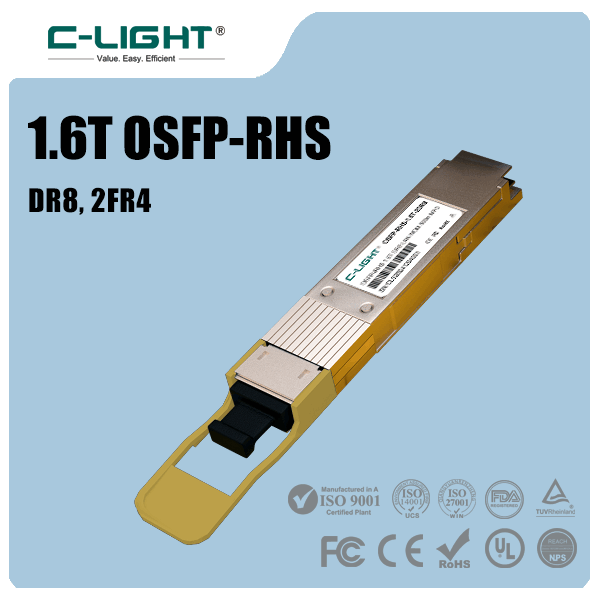
| 1.6T | Next-generation multi-lane architecture targeting 224G-class electrical signaling. | Higher-bandwidth circuits, advanced packaging, signal integrity and thermal density. |
These are general technology directions, not universal lane mappings. The exact electrical interface, optical channel arrangement, modulation format and DSP implementation must be confirmed against the specific module standard and datasheet.
13. Power and Thermal Management Affect Both Circuit Sections
Transmitter and receiver circuits operate at high speed, and their power consumption contributes to the module's total thermal load. Laser drivers, DSPs, CDRs, TIAs and other integrated circuits all generate heat during operation.
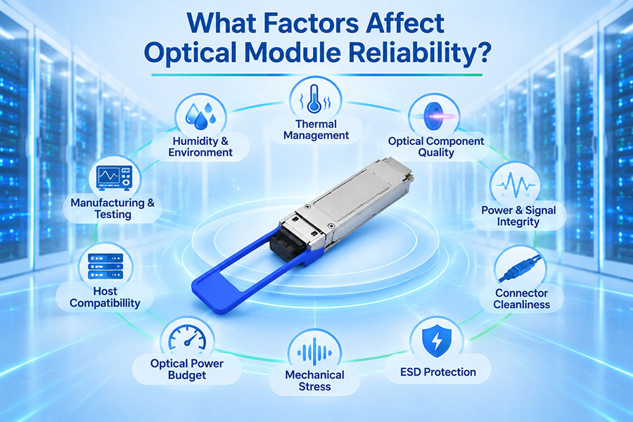
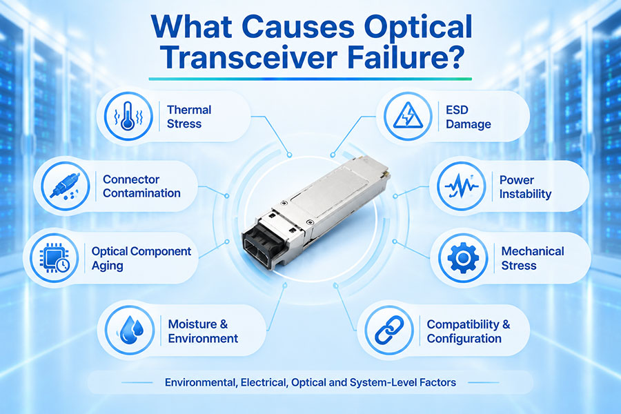
Temperature can influence laser threshold current, optical output, wavelength, photodetector behavior and electronic circuit characteristics. A module therefore needs an appropriate thermal design to keep its components within specified operating conditions.
Thermal management becomes particularly important in high-density switch platforms using 400G, 800G and 1.6T modules. The module's power rating, heatsink arrangement, host cage, airflow direction and chassis cooling capability must be considered together.
14. Common Circuit-Related Problems in Optical Modules
When an optical link experiences unstable performance, the fault may originate in the transmitter, receiver, host electrical interface or fiber channel. Diagnostic information and targeted testing help narrow down the source.
| Observed Symptom | Possible Circuit-Related Cause | Useful Diagnostic Focus |
|---|---|---|
| Low transmit optical power | Laser drive, bias control, optical source or coupling issue. | Check Tx power, laser bias and module operating conditions. |
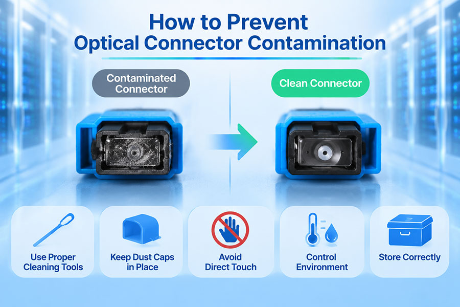
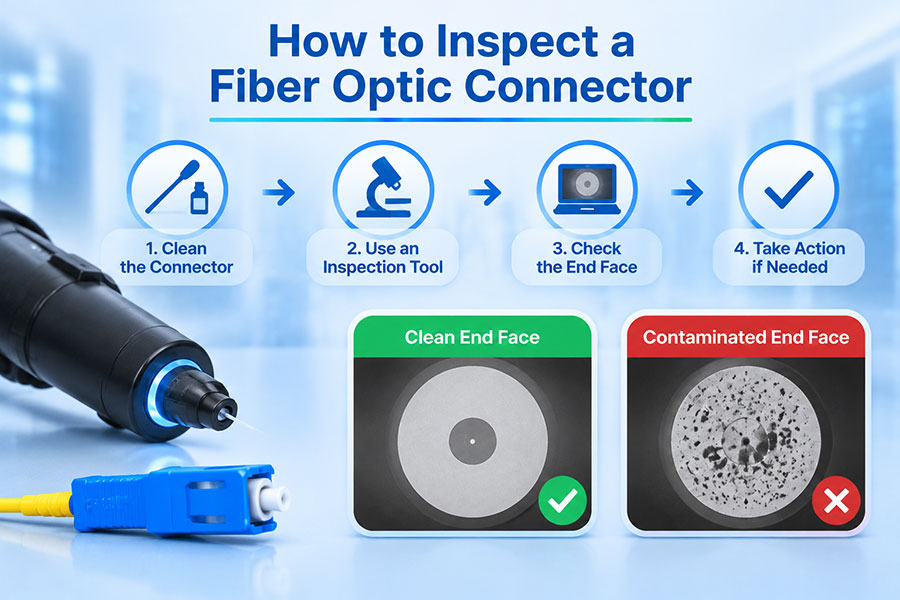
| Low received optical power | Receiver input level, fiber loss or optical coupling issue. | Check Rx power, connectors, fiber path and link budget. |
| High bit error rate | Signal distortion, noise, timing errors or insufficient optical margin. | Review BER, signal quality, optical power and host interface conditions. |
| Intermittent link operation | Thermal instability, power supply variation or electrical interface problems. | Review module alarms, temperature, supply voltage and host logs. |
| Module overheating | High circuit power, inadequate airflow or poor thermal contact. | Check module temperature, power consumption and chassis cooling. |
These symptoms are not definitive proof of a specific component failure. For example, low received power can result from fiber or connector loss rather than a defective receiver circuit. Diagnosis should consider the complete optical link and the host platform.
15. Applying Transmitter and Receiver Circuit Design to 400G Optical Modules
A 400G OSFP module brings the transmitter and receiver functions together in a high-density package intended for demanding data center and computing networks. Its circuit design must support high-speed electrical interfaces, optical conversion, module management and thermal requirements within the OSFP form factor.
C-LIGHT's 400G OSFP product family includes SR4, DR4, FR4 and LR4 configurations. The listed options cover multimode and single-mode fiber applications, with different wavelengths, connectors and transmission distances. These configurations provide practical examples of how optical source, receiver and interface requirements vary across module types.
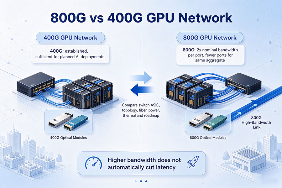
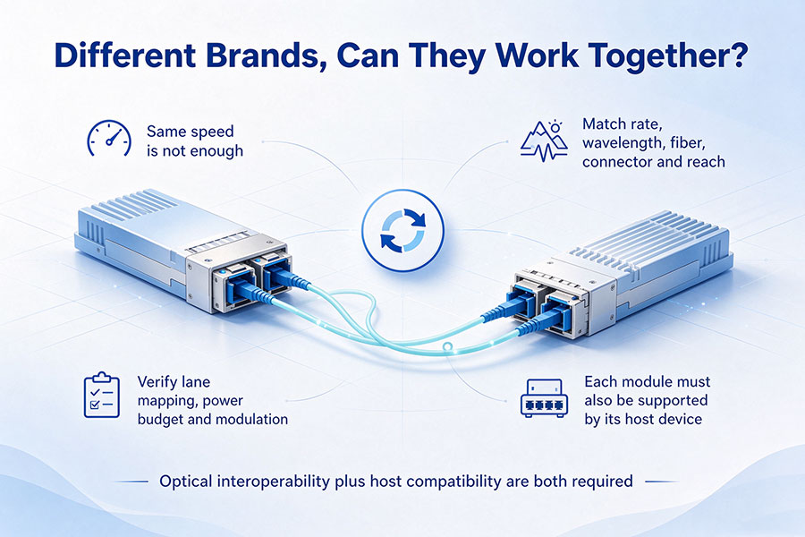
When selecting a module, engineers should verify its electrical interface, optical standard, host compatibility, connector type, fiber requirements, operating temperature and diagnostic capabilities. A shared 400G data-rate label does not mean that different optical interfaces or circuit implementations are interchangeable.
16. Conclusion
Transmitter and receiver circuits perform complementary roles inside an optical module. The transmitter uses input conditioning, laser drivers and optical sources to create a controlled optical signal. The receiver uses photodetectors, TIAs, amplification and timing recovery to reconstruct the transmitted electrical data.
Reliable operation depends on the coordination of these circuits with the optical interface, fiber channel, host SerDes and thermal environment. As data rates advance, improvements in driver performance, receiver sensitivity, signal processing, integration and power efficiency remain central to optical module development.
C-LIGHT provides optical transceiver solutions for data center, Ethernet, telecom and high-performance computing applications. For help selecting an optical module or checking equipment compatibility, Contact C-LIGHT.
 >

 >
 >
 >
 >
 >
 >
 >