TEL:+86 132 6656 7067





At 100G, 400G and 800G data rates, maintaining signal integrity requires careful control of both electrical and optical signal quality. A transceiver must receive clean electrical data from the host, convert it into a well-defined optical waveform, transmit that waveform through fiber and recover the original information at the receiving end. Distortion introduced at any stage can reduce the available operating margin and increase the bit error rate (BER).
Signal integrity is therefore not the result of a single circuit or component. It depends on the interaction between the host SerDes, module electrical interface, laser driver, optical source, fiber channel, photodetector, receiver amplifier and signal-processing circuitry. Optical transceivers maintain reliable transmission by controlling noise, jitter, reflections, attenuation, dispersion and thermal variation throughout this signal path.
1. What Signal Integrity Means in an Optical Transceiver
Signal integrity describes how accurately a transmitted signal preserves its intended electrical or optical characteristics as it travels through a communication system. A signal with good integrity can be detected and decoded reliably at the receiver. A degraded signal may contain excessive noise, timing variation, amplitude distortion or waveform interference.
Inside an optical transceiver, signal integrity has two closely related dimensions:
Electrical signal integrity: The quality of high-speed electrical signals traveling between the host device and the transceiver's internal circuits.
Optical signal integrity: The quality of the light transmitted through the fiber, including optical power, modulation characteristics, wavelength stability and resistance to transmission impairments.
Both dimensions matter. A clean optical transmitter cannot fully compensate for a severely degraded host electrical input, while a well-designed receiver cannot reliably recover data if the optical waveform has been excessively distorted.
2. How Signal Integrity Is Maintained Across the Transceiver
Signal integrity is managed at several stages of the transmission process. Each stage addresses a different source of signal degradation.
The transmitter controls the quality of the signal it launches. The optical channel determines how that signal changes during propagation. The receiver then compensates for supported impairments and reconstructs the transmitted data.
3. Electrical Channel Design Reduces Signal Distortion
Before electrical data reaches the optical components, it travels through the host PCB, connector contacts, module pads and internal high-speed traces. These structures form an electrical transmission channel with frequency-dependent loss and impedance characteristics.
At high data rates, even small discontinuities can affect the waveform. Poor impedance matching can cause reflections, while excessive insertion loss can reduce signal amplitude and distort transitions. Crosstalk from neighboring high-speed lanes can introduce additional interference.
Optical module and host designs address these problems through several measures:
Controlled impedance: High-speed differential traces and connectors are designed to maintain the intended characteristic impedance.
Short electrical paths: Compact routing reduces exposure to insertion loss and parasitic effects.
PCB layout control: Trace geometry, reference planes, via transitions and lane spacing are managed to limit discontinuities and crosstalk.
Return-path continuity: Proper grounding and reference-plane design help maintain predictable high-frequency current paths.
Connector performance: The host cage and module electrical interface must support the required signaling rate.
These considerations become increasingly important as electrical lane rates rise. A module may meet its optical specifications but still experience link errors if the host electrical channel does not provide sufficient signal quality.
4. Equalization Compensates for Electrical Channel Loss
High-speed electrical channels attenuate signal components differently across the frequency spectrum. This can cause pulse spreading and intersymbol interference (ISI), where energy from one transmitted symbol affects the detection of neighboring symbols.
Equalization compensates for part of this channel response. Depending on the implementation, equalization can be performed in the transmitter, receiver or both.
| Equalization Technique | Typical Location | Function |
|---|---|---|
| FFE – Feed-Forward Equalization | Transmitter or receiver DSP | Uses weighted signal samples to compensate for channel distortion. |
| CTLE – Continuous-Time Linear Equalizer | Receiver analog front end | Adjusts frequency response to compensate for channel loss. |
| DFE – Decision-Feedback Equalizer | Receiver | Uses previous symbol decisions to reduce post-cursor intersymbol interference. |
| DSP Equalization | Digital signal-processing section | Applies digital compensation according to the transceiver architecture. |
Equalization does not eliminate every source of distortion. It has finite compensation capability and can also amplify noise if applied excessively. The equalizer must therefore be configured for the actual channel rather than treated as a universal correction mechanism.
5. Clock and Data Recovery Controls Timing Accuracy
Even when a signal has sufficient amplitude, timing uncertainty can cause the receiver to sample it at the wrong moment. This timing variation is known as jitter.
Clock and data recovery (CDR) circuitry extracts timing information from the incoming data stream and establishes an appropriate sampling clock. Depending on the module architecture, CDR may also retime the data before it is delivered to the next stage.
CDR helps manage timing-related impairments, but its ability to tolerate jitter is limited by its design and operating conditions. Excessive jitter can close the eye opening and reduce the receiver's sampling margin.
Some modules use retimed architectures with dedicated CDR functions. Others use linear or low-power architectures that rely more heavily on the host SerDes and do not perform the same level of retiming inside the module.
6. Laser Driver Design Preserves Transmitter Signal Quality
The laser driver converts the incoming electrical data into controlled drive signals for the optical source or external modulator. Its performance directly influences the quality of the transmitted optical waveform.
Important transmitter design considerations include:
Bias current stability: Maintains the laser's operating point within its specified range.
Modulation accuracy: Controls the data-dependent changes in optical output.
Rise and fall characteristics: Supports sufficiently fast transitions without excessive waveform distortion.
Noise performance: Limits unwanted fluctuations introduced by the driver circuitry.
Thermal stability: Helps maintain consistent operating behavior as module temperature changes.
In directly modulated transmitters, the driver changes laser current to encode data. In externally modulated designs, a separate modulator changes light generated by a laser source. Both approaches require carefully controlled electrical drive conditions to meet the intended optical signal specifications.
7. Optical Power and Extinction Ratio Affect Signal Quality
After the electrical signal has been converted into light, the optical waveform must maintain sufficient power and suitable modulation characteristics. Two important transmitter parameters are average optical output power and extinction ratio.
Average optical output power indicates the average optical power launched by the transmitter. It must remain within the specified range so that the signal reaches the receiver with adequate margin without exceeding its maximum input limit.
Extinction ratio describes the relationship between the optical power levels representing different transmitted states. An appropriate extinction ratio helps distinguish signal levels at the receiver.
For multi-level modulation, additional waveform characteristics become important. PAM4 transmitters must maintain suitable linearity and separation among four amplitude levels. Distortion or noise can make those levels harder to distinguish, increasing the probability of symbol errors.
8. Fiber Quality and Optical Connections Preserve the Signal
After leaving the transmitter, light travels through fiber and passes through optical connections along the link. Fiber attenuation, connector loss, reflections and dispersion can all affect the received signal.
Several installation and component factors influence optical signal quality:
Fiber attenuation: Reduces received optical power as transmission distance increases.
Connector insertion loss: Reduces power at each connection point.
Connector reflections: Can return a portion of the optical signal toward the transmitter.
Fiber bending: Excessive bending can introduce additional optical loss.
Dispersion: Spreads optical pulses or symbols over time, potentially increasing intersymbol interference.
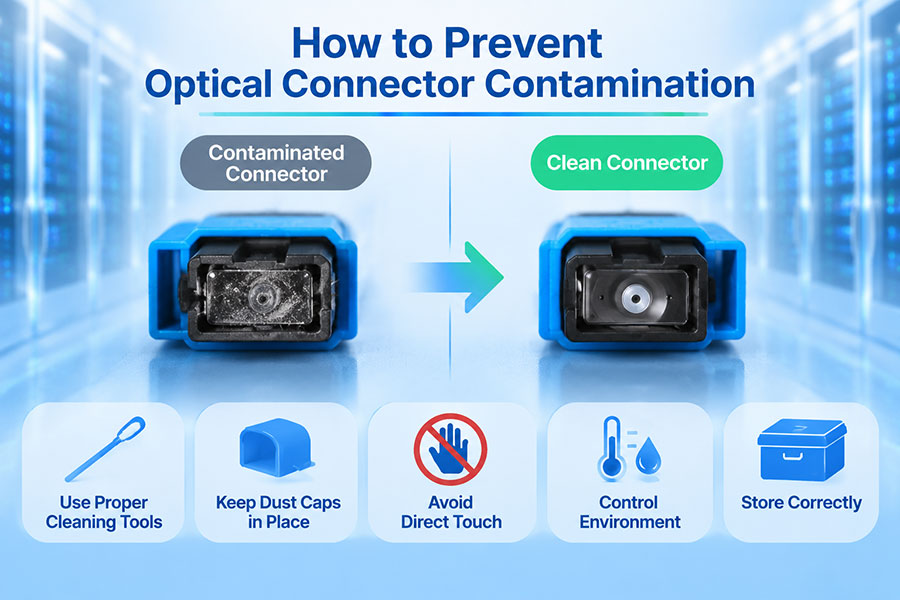
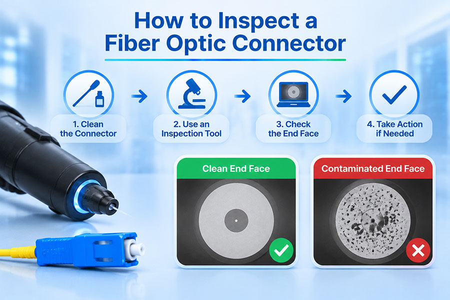
Contamination: Dust or residue on connector end faces can increase loss and back reflection.
Using the correct fiber category, maintaining connector cleanliness and following the specified bend-radius requirements help preserve the optical channel's performance.
9. Receiver Circuits Detect and Recover Weak Optical Signals
At the receiving end, a photodetector converts incoming light into photocurrent. A transimpedance amplifier (TIA) converts that small current into a voltage signal for subsequent receiver processing.
The receiver must amplify the signal without introducing excessive noise. It may then use additional amplification, filtering, equalization, CDR and DSP to recover the transmitted data.
Several receiver parameters are important:
| Receiver Parameter | Meaning | Signal Integrity Impact |
|---|---|---|
| Receiver Sensitivity | Minimum optical input power for specified performance. | Determines the receiver's ability to detect weak signals. |
| Overload Level | Maximum specified optical input level under defined conditions. | Prevents excessive input power from degrading receiver operation. |
| Receiver Bandwidth | Frequency range supported by the receiver. | Influences the ability to process high-speed signal transitions. |
| Input-Referred Noise | Noise contribution referred to the receiver input. | Affects the ability to distinguish signal levels. |
| Jitter Tolerance | Ability to recover data under timing variation. | Defines the timing margin available for reliable data recovery. |
A receiver's performance depends on the combined photodetector, TIA and signal-processing design. Improving one component does not automatically improve the complete receiver if another stage becomes the limiting factor.
10. PAM4 Requires Tighter Signal Integrity Control
PAM4 is widely used in modern high-speed optical modules because it carries two bits per symbol using four distinct amplitude levels. This increases the amount of information transmitted per symbol compared with NRZ, which uses two levels and carries one bit per symbol.
However, the four PAM4 levels have smaller vertical separation than a two-level NRZ signal under comparable amplitude conditions. Noise, nonlinear distortion and amplitude variation can therefore make adjacent levels more difficult to distinguish.
| Characteristic | NRZ | PAM4 |
|---|---|---|
| Signal levels | 2 | 4 |
| Bits per symbol | 1 | 2 |
| Amplitude separation | Two principal levels. | Four levels with smaller spacing under comparable signal swing. |
| Noise sensitivity | Generally more amplitude margin between decisions. | Requires tighter control of noise and level linearity. |
| Signal processing | Depends on the channel and data rate. | Often requires more advanced equalization and error management. |
PAM4 signal integrity is commonly evaluated using eye diagrams, signal-to-noise measurements, transmitter and receiver tests, and other standard-specific parameters. FEC may improve the system's ability to recover data from a certain level of errors, but it does not remove the underlying analog distortion.
11. Eye Diagrams Reveal Signal Quality
An eye diagram overlays many signal transitions within a common time interval. The resulting pattern provides a visual indication of timing and amplitude margins at a measurement point.
An open eye generally indicates more available decision margin, while a partially or fully closed eye suggests that noise, jitter, intersymbol interference or other impairments are reducing the receiver's ability to distinguish symbols.
Engineers use eye diagrams to evaluate several characteristics:
Eye height: Indicates vertical amplitude margin between signal decision levels.
Eye width: Indicates horizontal timing margin available for sampling.
Jitter: Appears as variation in the timing of signal transitions.
Noise: Appears as vertical spreading of signal levels.
Intersymbol interference: Can distort transitions and reduce the opening of the eye.
For PAM4 systems, the eye diagram contains three eye openings between the four signal levels. Each eye must meet the relevant requirements for the intended interface and operating conditions.
12. BER and FEC Help Evaluate Transmission Reliability
Bit error rate (BER) measures the proportion of received bits that differ from the transmitted bits during a defined test. It is one of the most important indicators of end-to-end digital transmission performance.
For example, if 10 erroneous bits are detected in 1 trillion received bits, the measured BER is 1 × 10-11.
Forward error correction (FEC) adds redundancy to transmitted data so that the receiver can correct certain errors. Different Ethernet and optical interfaces may specify different FEC methods and performance thresholds.
FEC improves error recovery within its correction capability, but it should not be treated as a substitute for adequate signal integrity. Excessive noise, distortion or optical loss can push a link beyond the correction capability of its FEC scheme.
When evaluating a transceiver, engineers should distinguish between pre-FEC BER and post-FEC BER. The former reflects errors before correction, while the latter indicates the remaining errors after the FEC process.
13. Thermal Management Helps Maintain Stable Signal Performance
High-speed optical modules contain laser drivers, DSPs, CDR circuits, TIAs and other electronic components that generate heat. Changes in temperature can affect laser characteristics, circuit timing, receiver behavior and overall operating stability.
Thermal management helps keep the module within its specified case-temperature range. The design may include a heat spreader, heatsink interface and airflow path appropriate for the module form factor and host platform.
Thermal design becomes especially important in high-density 400G, 800G and 1.6T network systems, where module power consumption and port density can create significant cooling demands.
Stable thermal conditions help reduce performance variation, but the module must still be validated across its specified operating temperature range rather than only under nominal laboratory conditions.
14. How Signal Integrity Is Tested Before Deployment
Signal integrity validation combines electrical, optical and system-level testing. No single measurement can establish the performance of the complete link under every operating condition.
| Test or Measurement | What It Evaluates | Typical Purpose |
|---|---|---|
| Eye Diagram | Amplitude and timing margin. | Identifies waveform distortion and reduced sampling margin. |
| BER Test | Digital transmission error performance. | Verifies whether the link meets the required error target. |
| TDECQ | Transmitter and dispersion eye closure penalty for applicable PAM4 interfaces. | Evaluates transmitter signal quality under defined measurement conditions. |
| Optical Power Measurement | Transmit and receive optical power. | Checks optical levels against module specifications. |
| Jitter Measurement | Timing variation in high-speed signals. | Evaluates clock and data recovery margin. |
| Temperature Testing | Performance across specified operating temperatures. | Checks thermal stability and operating margin. |
| Host Compatibility Testing | Electrical and management interoperability. | Verifies operation with the intended switch or network platform. |
For high-speed modules, test conditions must match the relevant interface specification. Measurement bandwidth, reference points, test patterns, FEC settings and environmental conditions can all influence the results.
15. Applying Signal Integrity Principles to 400G Optical Modules
A 400G optical module demonstrates how electrical and optical signal integrity requirements come together in a high-bandwidth transceiver. The host interface, lane architecture, modulation format, transmitter and receiver circuits, fiber connection and thermal design must operate as a coordinated system.
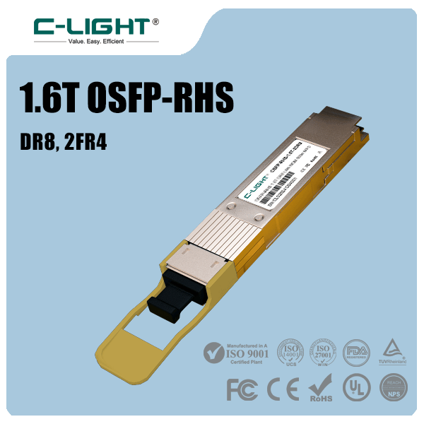
C-LIGHT's 400G OSFP family supports multiple optical configurations, including SR4, DR4, FR4 and LR4 options. The product family is designed for AI data centers, cloud computing and high-performance computing applications. Its listed specifications include different fiber types, optical reaches and connector interfaces for different deployment requirements.
When evaluating a 400G module, engineers should verify the exact part number, host electrical interface, optical standard, modulation requirements, FEC configuration and thermal conditions.
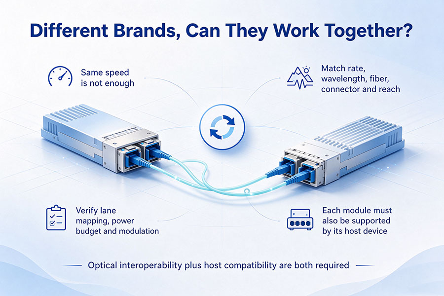
In a real deployment, the optical module should be evaluated together with the host switch or adapter and the installed fiber channel. Matching the nominal data rate is not enough: the electrical interface, optical specification, connector, fiber type and system configuration must also be compatible.
16. Conclusion
An optical transceiver maintains signal integrity by controlling signal quality throughout the electrical and optical transmission path. Electrical channel design, equalization and CDR help preserve the host signal, while laser drive control and optical source performance determine the quality of the transmitted light. Fiber management, receiver sensitivity, low-noise amplification and digital signal processing then support reliable data recovery.
As PAM4 and higher per-lane signaling rates become common in 400G, 800G and 1.6T networks, signal integrity requires increasingly careful coordination among electrical design, photonic components, optical interfaces and thermal management. Eye diagrams, BER measurements and standard-specific optical and electrical tests are essential for validating performance.
C-LIGHT provides optical transceiver solutions for data center, Ethernet, telecom and high-performance computing applications. For assistance with module selection, equipment compatibility or high-speed optical connectivity requirements, Contact C-LIGHT.
 >

 >
 >
 >
 >
 >
 >
 >