TEL:+86 132 6656 7067





Fiber-optic communication depends on a conversion process that allows electronic networking equipment to exchange data through light. Switches, routers, servers, and network interface cards process information as electrical signals, while optical fiber carries information through modulated light. An optical transceiver connects these two domains by converting outgoing electrical data into optical signals and incoming optical signals back into electrical data.
This process involves several coordinated components, including a laser driver, semiconductor light source, optical coupling assembly, photodetector, transimpedance amplifier, and, in many high-speed designs, clock and data recovery or digital signal processing circuits. The exact implementation varies with data rate, transmission distance, wavelength, modulation format, and transceiver architecture.
Understanding the electrical-to-optical conversion process helps explain why optical modules require careful matching with host equipment, fiber types, link distances, and operating conditions.
1. The Basic Working Principle of an Optical Transceiver
An optical transceiver performs two complementary functions: transmission and reception. The transmitter converts an electrical data stream into a modulated optical signal, while the receiver detects incoming light and reconstructs the corresponding electrical data.
These functions are commonly implemented in two internal assemblies:
TOSA (Transmitter Optical Sub-Assembly): Generates and couples the outgoing optical signal into the fiber.
ROSA (Receiver Optical Sub-Assembly): Detects incoming optical signals and converts them into electrical signals.
In a conventional duplex optical transceiver, the transmit and receive paths operate through separate optical interfaces. The transmitter sends light through one fiber, while the receiver detects light arriving through another. Single-fiber bidirectional modules use different wavelengths to transmit and receive through the same fiber.
2. How the Transmitter Converts Electrical Signals into Light
The transmission process begins when a switch, router, or server sends electrical data to the optical module through its host electrical interface. The module then prepares the signal for optical transmission.
Depending on the module architecture, the signal may pass through equalization, clock recovery, retiming, digital signal processing, or other conditioning functions before reaching the optical transmitter.
The main conversion stages are outlined below.
Stage 1: Electrical Signal Input
The host device sends high-speed electrical signals through the module's electrical contacts. These signals represent the data stream that must be transmitted across the optical link.
Modern optical modules commonly use differential electrical signaling. The signal format and lane configuration depend on the module's form factor and data rate. For example, a high-speed 400G or 800G module may use multiple electrical lanes operating in parallel.
Before reaching the laser driver, the electrical signal may require conditioning to compensate for channel loss, timing variation, and other transmission impairments.
Stage 2: Signal Processing and Conditioning
High-speed electrical channels experience attenuation, reflections, crosstalk, and timing distortion as signals travel through host circuit boards and module interfaces. Signal-processing circuits help maintain the quality of the data presented to the optical transmitter.
Depending on the design, this stage may include:
Equalization: Compensates for frequency-dependent signal loss.
Clock and Data Recovery (CDR): Extracts timing information and helps restore signal timing.
Digital Signal Processing (DSP): Performs functions such as equalization, modulation-related processing, and signal compensation in applicable architectures.
Retiming: Reconstructs signal timing before transmission when supported by the module design.
Not every optical transceiver contains all these functions. Some designs use a DSP, while others use a linear electrical interface or simpler signal-conditioning architecture. The implementation depends on the application and the required electrical and optical performance.
Stage 3: Laser Driver Controls the Light Source
After signal conditioning, the electrical data reaches the laser driver. This circuit supplies the controlled electrical current required to operate the semiconductor laser or other optical transmitter.
In a directly modulated laser design, the driver changes the laser current according to the incoming data. This causes the emitted optical power to vary in accordance with the transmitted signal.
In an externally modulated design, the laser can provide a relatively continuous optical carrier, while a separate modulator changes the optical signal according to the electrical data. Electro-absorption modulators and Mach-Zehnder modulators are examples of technologies used in different optical systems.
The laser driver must provide accurate control of signal amplitude, bias conditions, and modulation behavior. Poor driver performance can reduce optical signal quality and contribute to transmission errors.
Stage 4: Semiconductor Laser Generates Optical Signals
The semiconductor laser is the component that generates the light used for optical communication. When driven by an appropriate electrical current, it produces optical energy at a wavelength selected for the intended application.
Several types of light sources are used in optical transceivers:
| Light Source | Operating Principle | Typical Applications |
|---|---|---|
| VCSEL | Emits light perpendicular to the semiconductor surface. | Short-reach multimode optical links, including many 850nm applications. |
| DFB Laser | Uses a distributed feedback structure to provide wavelength-selective laser emission. | Single-mode optical links and wavelength-specific transmission systems. |
| EML | Combines a laser source with an electro-absorption modulator. | High-speed single-mode applications requiring external optical modulation. |
| Other externally modulated sources | Use a separate optical modulator to encode electrical data onto light. | High-performance and specialized optical transmission systems. |
The laser wavelength, output power, modulation capability, and spectral characteristics must match the intended optical interface. For example, an 850nm VCSEL-based transmitter is commonly associated with multimode fiber, while many single-mode data center transceivers use 1310nm optical sources.
Stage 5: Optical Coupling Sends Light into the Fiber
Generating light inside the module is only part of the transmission process. The optical signal must also be coupled efficiently into the fiber.
The transmitter assembly uses optical components such as lenses, alignment structures, and fiber interfaces to guide the emitted light toward the fiber core. The coupling arrangement depends on the optical source, fiber type, and module design.
Alignment is important because optical coupling losses reduce the power launched into the fiber. The transmitter must deliver sufficient optical power while remaining within the specified output and safety limits of the optical interface.
3. How the Receiver Converts Light Back into Electrical Signals
At the receiving end, the optical transceiver performs the reverse conversion. Light arriving through the fiber enters the receiver assembly, where a photodetector converts optical energy into an electrical current.
The resulting electrical signal is initially weak and requires amplification and signal processing before it can be delivered to the host device.
Stage 1: Optical Signal Reception
The incoming optical signal passes through the receiver's optical interface and is directed toward the photodetector. The receiver must detect the optical signal across the specified wavelength and power range.
Optical power at the receiver depends on several factors, including transmitter output power, fiber attenuation, connector losses, splices, and other channel impairments.
Stage 2: Photodiode Converts Light into Electrical Current
The photodiode is the key optical-to-electrical conversion component. When photons reach its photosensitive region, they generate charge carriers, producing a current related to the received optical power.
Two common photodetector types are PIN photodiodes and avalanche photodiodes.
| Photodetector | Operating Principle | Characteristics |
|---|---|---|
| PIN Photodiode | Converts incident photons into electrical current through the photoelectric effect. | Common receiver technology with relatively simple operation and good linearity. |
| APD | Uses internal avalanche multiplication to increase the electrical response generated by incoming light. | Can provide higher sensitivity in suitable applications but requires additional bias and control considerations. |
The choice of photodetector depends on the required receiver sensitivity, data rate, wavelength, optical reach, and overall receiver architecture.
Stage 3: Transimpedance Amplifier Converts Current into Voltage
The electrical current generated by the photodiode is generally too small to be processed directly by the host interface. A Transimpedance Amplifier (TIA) converts this current into a voltage signal and provides the necessary amplification.
The TIA is a critical part of the ROSA because its noise performance, bandwidth, gain, and linearity influence the receiver's ability to distinguish the incoming data signal.
At high data rates, the receiver must preserve signal quality across a wide frequency range. TIA design therefore has a direct impact on sensitivity and overall link performance.
Stage 4: Signal Amplification, Recovery and Processing
After the TIA, additional receiver circuits process the electrical signal. Depending on the transceiver architecture, these may include limiting amplifiers, equalizers, CDR circuits, and DSP functions.
Limiting amplifier: Provides a controlled output amplitude for suitable receiver architectures.
Equalizer: Compensates for signal distortion and frequency-dependent loss.
CDR: Recovers timing information and reconstructs the data stream.
DSP: Performs additional signal processing when required by the modulation format and link design.
Once the signal has been processed, the receiver sends the reconstructed electrical data through the module's host interface to the switch, router, or server.
4. TOSA and ROSA: The Two Main Optical Conversion Assemblies
TOSA and ROSA are the core optical assemblies responsible for the transmitter and receiver functions. They are designed to work with the module's electrical circuits and optical interfaces.
| Feature | TOSA | ROSA |
|---|---|---|
| Full Name | Transmitter Optical Sub-Assembly | Receiver Optical Sub-Assembly |
| Main Function | Electrical-to-optical conversion | Optical-to-electrical conversion |
| Key Components | Laser diode, optical coupling components, and associated transmitter elements. | Photodiode, optical interface, and receiver components. |
| Electrical Circuit | Works with a laser driver. | Works with a TIA and subsequent receiver circuitry. |
| Signal Direction | Electrical input to optical output. | Optical input to electrical output. |
In many conventional module architectures, TOSA and ROSA are identifiable internal assemblies. In highly integrated transceivers, however, optical and electronic functions may be combined into more compact optical engine or photonic integrated circuit designs.
The underlying conversion functions remain necessary even when the physical implementation changes.
5. How NRZ and PAM4 Modulation Affect Optical Conversion
Electrical-to-optical conversion does not always use the same signaling format. The modulation method determines how data is represented in the optical signal and influences the transmitter, receiver, and signal-processing requirements.
NRZ and PAM4 are two important modulation formats used in optical communication.
| Characteristic | NRZ | PAM4 |
|---|---|---|
| Signal Levels | 2 amplitude levels | 4 amplitude levels |
| Bits per Symbol | 1 bit | 2 bits |
| Data Representation | Two signal levels represent binary data. | Four signal levels represent two bits per symbol. |
| Receiver Requirements | Distinguishes between two signal levels. | Must distinguish among four signal levels with tighter amplitude and noise margins. |
| Typical Context | Many traditional lower-rate optical interfaces. | Many modern 50G-per-lane and 100G-per-lane optical interfaces. |
PAM4 increases the number of bits represented by each symbol, allowing higher data rates without requiring the symbol rate to increase by the same factor as NRZ. However, the four signal levels are closer together than the two levels used in NRZ, making the receiver more sensitive to noise and signal distortion.
This is one reason high-speed PAM4 transceivers often require more advanced equalization, DSP, and error-correction strategies. The optical transmitter must generate distinguishable signal levels, and the receiver must recover the transmitted information with sufficient accuracy.
6. How Multi-Lane Optical Transceivers Increase Bandwidth
Modern high-speed optical modules often use multiple parallel electrical and optical lanes to achieve higher aggregate bandwidth. Rather than transmitting the entire data stream through one high-speed optical channel, the module distributes data across several lanes.
For example, a 400G optical transceiver may use four or eight electrical lanes depending on its architecture. The optical side may use parallel fibers, multiple wavelengths, or a combination of optical technologies.
| Module Class | Representative Lane Architecture | Aggregate Data Rate |
|---|---|---|
| 100G | 4 × 25G NRZ or 1 × 100G PAM4, depending on implementation | 100Gbps |
| 200G | 4 × 50G PAM4 or other supported lane arrangements | 200Gbps |
| 400G | 8 × 50G PAM4 or 4 × 100G PAM4, depending on implementation | 400Gbps |
| 800G | 8 × 100G PAM4 in common implementations | 800Gbps |
| 1.6T | 8 × 200G-class electrical lanes in emerging designs | 1.6Tbps |
These are representative architectures rather than universal lane mappings. Actual implementations depend on the applicable Ethernet or InfiniBand standard, module form factor, electrical interface, and optical design.
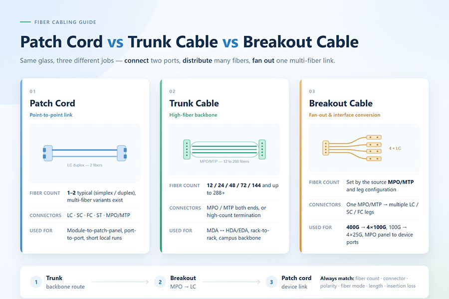
Multi-lane transmission also makes optical mapping important. Each electrical lane must be correctly associated with its corresponding optical channel or wavelength. Incorrect lane mapping, fiber polarity, or breakout configuration can prevent a link from operating properly even when the module is physically installed.
7. What Happens Inside Different Optical Transceiver Form Factors?
The electrical-to-optical conversion principle is broadly similar across SFP, SFP28, QSFP28, QSFP-DD, OSFP, and other optical module form factors. Their differences are mainly related to mechanical dimensions, electrical lane configuration, data rate, power requirements, thermal design, and optical interface implementation.
| Form Factor | Common Applications | Design Characteristics |
|---|---|---|
| SFP | 1G and other supported lower-rate interfaces. | Compact single-lane pluggable architecture. |
| SFP28 | 25G Ethernet and related applications. | Higher-speed single-lane electrical interface. |
| QSFP28 | 100G optical networking. | Four-lane electrical architecture in common implementations. |
| QSFP-DD | 400G and supported lower-rate applications. | Double-density electrical interface with multiple high-speed lanes. |
| OSFP | 400G, 800G, and supported high-speed applications. | High-density form factor with thermal and electrical designs suited to higher bandwidth. |
Although the internal optical conversion process follows the same general principles, the components are not automatically interchangeable across form factors. Mechanical dimensions, host electrical interfaces, management protocols, power limits, and optical standards must all be compatible.
8. Factors That Affect Electrical-to-Optical Conversion Performance
The quality of the conversion process affects the reliability and performance of the entire fiber-optic link. Several parameters determine how effectively an optical module transmits and receives data.
Transmitter output power: Determines the optical power launched into the fiber.
Receiver sensitivity: Indicates the minimum received optical power required to achieve a specified performance level.
Extinction ratio: Describes the optical power difference between logical signal states in applicable modulation formats.
Wavelength accuracy: Helps ensure that the optical signal operates within the specified wavelength range.
Optical coupling loss: Reduces the power delivered from the optical source into the fiber.
Electrical signal integrity: Affects the quality of the signal driving the optical transmitter and the signal recovered by the receiver.
Thermal stability: Influences laser characteristics, receiver performance, and overall module operation.
Noise and distortion: Can reduce the receiver's ability to distinguish transmitted signal levels.
These parameters are evaluated through optical and electrical testing. Depending on the module type, testing may include transmit power, receiver sensitivity, extinction ratio, eye diagrams, bit error ratio, and digital diagnostic monitoring.
9. C-LIGHT Optical Transceiver Solutions for High-Speed Networks
The electrical-to-optical conversion process is used across a wide range of networking applications, from conventional Ethernet links to high-bandwidth AI data center fabrics. Different applications require different module architectures, optical sources, fiber interfaces, and transmission distances.
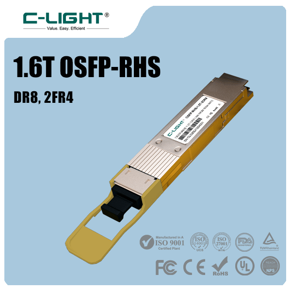
C-LIGHT provides optical transceiver solutions across multiple data rates and form factors, including 25G SFP28, 100G QSFP28, 400G OSFP, 400G QSFP-DD, 800G OSFP, and 1.6T OSFP platforms.
Example: C-LIGHT 400G OSFP Optical Transceiver
The C-LIGHT 400G OSFP optical transceiver is designed for AI data centers, cloud computing networks, and high-performance computing systems.
The product uses a high-speed multi-lane electrical interface and supports optical configurations including SR4, DR4, and FR4. These configurations address different fiber types and transmission distances, allowing the module to be selected according to the requirements of the network link.
400Gbps aggregate transmission capability.
OSFP form factor.
Support for applicable IEEE and InfiniBand NDR environments.
Multiple optical reach configurations.
Designed for high-bandwidth data center and HPC connectivity.
The product illustrates how electrical lane processing, optical transmission, and multi-channel design work together inside a modern high-speed transceiver.
For other applications, C-LIGHT's optical transceiver portfolio includes modules for Ethernet, InfiniBand, Fibre Channel, PON, CWDM, DWDM, and data center interconnect networks. The correct product should be selected according to the host interface, data rate, optical reach, wavelength, fiber type, and connector requirements.
10. Conclusion
An optical transceiver converts electrical signals into optical signals through a coordinated transmitter process involving signal conditioning, a laser driver, a semiconductor light source, and optical coupling components. At the receiving end, a photodetector converts incoming light into electrical current, which is amplified and processed before being delivered to the host device.
TOSA and ROSA are the central optical assemblies behind these two conversion directions. Their performance depends on the quality of the laser or photodetector, driver and amplifier circuits, optical alignment, modulation format, and thermal design.
As networking speeds increase from 100G and 400G to 800G and 1.6T, optical transceivers require more advanced electrical interfaces, multi-lane architectures, and signal-processing technologies. Understanding the conversion process makes it easier to evaluate optical module specifications, diagnose link issues, and select suitable transceivers for modern fiber-optic networks.
Looking for optical transceivers for your network application?
C-LIGHT provides optical modules for data centers, Ethernet networks, telecommunications, and high-performance computing. Contact the team for product specifications, compatibility support, and optical connectivity solutions.
 >

 >
 >
 >
 >
 >
 >
 >