TEL:+86 132 6656 7067





How Does an APD Improve Optical Receiver Sensitivity?
In long-distance fiber-optic links, the optical signal can become extremely weak after passing through fiber attenuation, connectors, splices, and other optical components. The receiver must still distinguish the incoming data from electrical noise and recover it with an acceptable bit error rate (BER). When the photocurrent generated by a conventional photodiode is too small relative to the receiver amplifier's noise, an avalanche photodiode (APD) can provide an important sensitivity advantage.
An APD improves detection by generating internal electrical gain through impact ionization. Instead of relying entirely on the small photocurrent produced by incoming photons, it multiplies the primary carriers inside the semiconductor before the signal reaches the following amplification stage. This can improve the receiver's signal-to-noise ratio, provided that avalanche noise and other limitations remain under control.
1. What Is an Avalanche Photodiode?
An avalanche photodiode is a semiconductor optical detector that converts incident light into electrical current and provides internal multiplication gain. Like a PIN photodiode, it absorbs photons and generates electron-hole pairs. Its distinguishing feature is a high electric field in the multiplication region, where accelerated carriers can generate additional electron-hole pairs through impact ionization.
This multiplication process increases the electrical output generated by a given optical input. The resulting current is therefore larger than the primary photocurrent produced by the absorbed light alone.
APDs are used in optical receivers where detecting weak signals is especially important. Depending on the device structure, semiconductor materials, wavelength, and operating conditions, they can support sensitive optical detection in fiber communication and other photonic systems.
2. How Does the Avalanche Multiplication Process Work?
The APD operates under reverse bias. When an incoming photon is absorbed in the photodetection region, it generates an electron-hole pair. The electric field accelerates the carriers, and carriers entering the multiplication region may gain enough energy to trigger impact ionization.
During impact ionization, an energetic carrier transfers energy to the semiconductor lattice and generates another electron-hole pair. The newly generated carriers can also be accelerated and create further carriers. This chain of events produces the avalanche multiplication effect.
The process can be understood in four stages:
Photon absorption: Incoming optical energy generates primary electron-hole pairs in the semiconductor.
Carrier acceleration: The reverse-bias electric field drives the carriers through the device.
Impact ionization: Energetic carriers generate additional electron-hole pairs in the multiplication region.
Current multiplication: The additional carriers increase the output photocurrent delivered to the receiver electronics.
The multiplication is an internal semiconductor process. It does not mean that the APD creates additional optical power or amplifies the light traveling through the fiber.
3. How Does APD Gain Improve Receiver Sensitivity?
Optical receiver sensitivity is the minimum optical power required at the receiver input to achieve a specified performance target, commonly defined by a particular BER, data rate, modulation format, and test condition.
A PIN photodiode produces a photocurrent proportional to the received optical power. At low input power, this current may be comparable to the noise contributed by the transimpedance amplifier (TIA) and other receiver electronics. The electrical signal can then become difficult to distinguish reliably.
An APD increases the primary photocurrent through its internal multiplication gain. Because this gain occurs before the following amplifier, it can make the optical signal more prominent relative to amplifier noise.
Where:
IAPD: Output photocurrent after avalanche multiplication.
Iprimary: Photocurrent generated before internal multiplication.
M: Average avalanche multiplication factor.
For example, if a detector generates a primary photocurrent of 1 μA and operates at an average multiplication factor of 10, its multiplied photocurrent is approximately 10 μA. This illustrates the current gain, not a tenfold improvement in receiver sensitivity. Actual sensitivity improvement depends on avalanche noise, amplifier noise, bandwidth, and the required BER.
4. The Relationship Between APD Gain and Signal-to-Noise Ratio
Increasing the photocurrent does not automatically produce an equal improvement in signal-to-noise ratio (SNR). The avalanche process is statistical: carriers do not all undergo exactly the same number of multiplication events. This randomness introduces additional noise, commonly called avalanche excess noise.
At relatively low multiplication gain, the stronger output signal can improve SNR because the contribution of downstream amplifier noise becomes less significant. As gain increases, however, avalanche-related noise also rises. Eventually, further multiplication provides diminishing returns and may reduce overall receiver performance.
The APD must therefore operate at a suitable multiplication factor rather than simply maximizing gain. The optimum value depends on the detector's ionization characteristics and the receiver's electronic noise.
5. What Is the APD Excess Noise Factor?
The excess noise factor describes the additional noise caused by the statistical variation of avalanche multiplication. It is commonly represented by F(M), where M is the average multiplication gain.
For a simplified conventional APD model, the relationship can be expressed as:
Here, k represents the ratio of the electron and hole impact-ionization coefficients, according to the model's material and carrier convention. The exact relationship depends on APD structure and the physical assumptions used.
A lower excess noise factor is generally desirable because it allows the APD to provide useful internal gain with less additional noise. Semiconductor material, multiplication-region design, and carrier transport characteristics all influence this behavior.
APD receiver design must balance three factors:
Enough multiplication gain to overcome a significant portion of the amplifier noise.
Low enough excess noise to preserve the SNR advantage.
Sufficient bandwidth and linearity for the required data rate and signal format.
6. APD vs. PIN Photodiode: Key Receiver Differences
Both APD and PIN photodiodes convert optical signals into electrical current, but their internal gain mechanisms lead to different receiver characteristics. A PIN photodiode has approximately unity internal gain, while an APD provides multiplication before the signal reaches the TIA.
| Parameter | PIN Photodiode | APD |
|---|---|---|
| Internal gain | No avalanche multiplication; gain is approximately unity | Provides internal multiplication gain |
| Weak-signal detection | Performance depends strongly on detector responsivity and receiver amplifier noise | Can improve detection when downstream electronic noise is a major limitation |
| Noise characteristics | Photocurrent shot noise, dark current noise, and receiver circuit noise | Includes additional avalanche excess noise |
| Bias requirements | Generally simpler bias arrangement | Requires carefully controlled reverse bias near the avalanche operating region |
| Temperature sensitivity | Device characteristics vary with temperature | Multiplication gain can be particularly sensitive to temperature and bias conditions |
| Receiver complexity | Usually simpler detector bias and control | Requires additional gain and bias management |
| Typical design priority | Low complexity, power efficiency, and suitable sensitivity | Improved weak-signal detection where internal gain provides a net benefit |
Neither detector is universally better. A well-designed PIN receiver can outperform an APD receiver in applications where amplifier noise is already low or where avalanche noise, bias complexity, and power consumption outweigh the potential sensitivity gain.
7. Why Does APD Bias Voltage Need Precise Control?
APD multiplication depends on the electric field inside the semiconductor. The reverse-bias voltage therefore has a direct influence on the avalanche gain. A small change in bias can cause a meaningful change in multiplication, especially when the device operates close to its breakdown region.
Temperature also affects the avalanche process. As temperature changes, carrier transport and impact-ionization characteristics change, which can shift the multiplication factor at a fixed bias voltage.
To maintain stable receiver performance, an APD design may use:
Low-noise bias generation: Reduces electrical noise coupled into the detector's operating voltage.
Temperature compensation: Adjusts the bias according to temperature to help maintain the target multiplication gain.
Gain monitoring: Uses device or receiver feedback to maintain a stable operating point where supported by the design.
Thermal management: Keeps the detector within its specified operating conditions.
Bias stability is especially important in receivers designed for weak optical signals. Uncontrolled gain variation can change the output level and noise behavior, making it harder to maintain consistent BER performance.
8. Where Are APDs Used in Optical Communication Systems?
APDs are particularly useful when the receiver must detect weak optical signals and the receiver's electronic noise is a significant part of the total noise budget. Their internal gain can help extend the usable optical link budget without requiring the detector itself to receive a stronger signal.
Typical application areas include:
Long-distance optical links: APD receivers can be useful in systems where received optical power is low and additional sensitivity is required.
Optical access networks: Certain receiver designs use APDs to meet sensitivity requirements under specific link-budget and cost constraints.
Digital optical communication: APDs can support data reception when the balance between electronic noise and avalanche noise favors internal multiplication.
Free-space optical communication: Weak received optical signals can make detector sensitivity an important system consideration.
APD use is not determined by transmission distance alone. The link budget, optical amplification, data rate, modulation format, receiver architecture, and total noise environment all influence detector selection.
9. What Limits APD Performance in High-Speed Receivers?
Although APDs can improve sensitivity, their design involves several trade-offs. The multiplication region and carrier transport must support the required bandwidth, while the receiver must manage the additional noise and bias requirements.
| Performance factor | Potential limitation | Design consideration |
|---|---|---|
| Multiplication gain | Higher gain also increases avalanche excess noise | Determine an optimum gain for the complete receiver |
| Gain-bandwidth product | Higher multiplication can reduce available bandwidth | Match the detector structure to the required data rate |
| Temperature variation | Gain may shift as operating temperature changes | Use suitable bias compensation and thermal design |
| Dark current | Contributes to receiver noise, particularly at high gain | Evaluate detector quality and operating conditions |
| Bias circuitry | Additional voltage generation and control increase complexity | Use a stable, low-noise bias architecture |
| Linearity and overload | Strong input signals can move the receiver outside its intended operating range | Check dynamic range and overload behavior |
In high-speed systems, detector sensitivity must be considered together with bandwidth, TIA performance, equalization, clock recovery, and the selected modulation format. A detector that provides high gain but cannot maintain the required bandwidth will not necessarily improve the complete link.
10. How Does an APD Affect the Optical Link Budget?
The optical link budget establishes how much optical power is available at the receiver after accounting for transmitter output power, fiber attenuation, connector losses, splice losses, and other optical impairments.
Receiver sensitivity determines the minimum acceptable received optical power for the specified BER. A more sensitive receiver can provide additional margin between the actual received power and the minimum required level.
For example, if a link delivers a weak signal close to the receiver's sensitivity limit, an APD may improve the detection margin when its internal gain reduces the impact of electronic noise. However, the APD's sensitivity advantage must be established using the complete receiver specification rather than inferred from its multiplication factor alone.
APD gain does not reduce fiber attenuation, connector insertion loss, or dispersion. It improves electrical detection after the optical signal reaches the photodiode. Link engineering must still account for all optical and electrical impairments.
11. How Is APD Receiver Sensitivity Tested?
Receiver sensitivity testing determines the minimum optical input power at which a receiver can maintain the required BER under defined operating conditions. For an APD receiver, the test must also account for its bias voltage, multiplication gain, and temperature behavior.
A typical evaluation considers:
Optical input power: The calibrated optical power delivered to the receiver reference point.
Bit error rate: The measured error performance at the specified data rate and signal format.
APD operating point: The bias and multiplication conditions used during the test.
Temperature: Performance across the specified operating temperature range.
Receiver bandwidth: Whether the detector and following electronics support the target signal rate.
Overload performance: The receiver's behavior when the optical input exceeds its intended operating level.
For high-speed PAM4 systems, sensitivity testing must follow the applicable interface specification and account for the relevant FEC and BER measurement definitions. Pre-FEC and post-FEC BER are different performance indicators and should not be treated as interchangeable.
12. APD Technology and High-Speed Optical Transceiver Design
Detector selection in modern optical transceivers is a system-level decision. An APD can be valuable when internal gain provides a measurable improvement in receiver sensitivity, but a PIN photodiode may be more suitable when the receiver already has sufficiently low electronic noise, or when power consumption, integration, and operating simplicity are higher priorities.
As data rates increase, the receiver must satisfy more than a minimum optical power requirement. Detector bandwidth, TIA noise, signal linearity, modulation format, FEC behavior, thermal stability, and host electrical interface performance all contribute to the final link result.
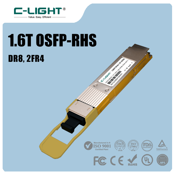
For example, C-LIGHT's 800G 1DR4 500m OSFP-RHS optical transceiver is a high-speed single-mode product example using an EML transmitter and PIN-based receiver detection architecture. It illustrates that high-speed receiver design does not automatically require APD technology; detector choice depends on the complete optical and electrical performance targets.
For network designers evaluating high-speed optical connectivity, C-LIGHT's optical transceiver portfolio provides a starting point for reviewing available module form factors and transmission applications. Specific detector type, receiver sensitivity, and operating limits should always be confirmed against the relevant product datasheet.
13. Conclusion
An avalanche photodiode improves optical receiver sensitivity through internal carrier multiplication. By increasing the photocurrent before it reaches the TIA, an APD can reduce the relative influence of downstream electronic noise and improve the detection of weak optical signals.
The benefit is not unlimited. Avalanche multiplication introduces excess noise, and higher gain can affect bandwidth, temperature stability, and bias requirements. The best operating point is therefore a balance between useful signal gain and the additional noise generated inside the detector.
For optical communication systems, APD and PIN photodiodes serve different receiver design priorities. Selecting the right detector requires evaluating the complete receiver architecture, optical link budget, data rate, BER target, and operating environment. For application or product selection support, Contact C-LIGHT.
 >

 >
 >
 >
 >
 >
 >
 >