TEL:+86 132 6656 7067




AI data centers are placing unprecedented demands on network bandwidth. As GPU and accelerator clusters become larger, the electrical connections between switching silicon, optical engines and network interfaces face increasing bandwidth, power and signal-integrity challenges.
Silicon photonics is becoming an important technology for addressing these requirements by integrating optical functions onto silicon-based photonic integrated circuits. Instead of relying entirely on discrete optical components, silicon photonics can bring lasers, modulators, photodetectors, waveguides and related optical functions into a more integrated architecture.
This approach is increasingly relevant to 800G and emerging 1.6T connectivity, as well as to co-packaged optics, near-packaged optics and next-generation AI networking architectures.
1. What Is Silicon Photonics?
Silicon photonics uses silicon-based integrated photonic structures to guide, modulate and detect optical signals.
A silicon photonic chip can contain optical waveguides, modulators, photodetectors and other photonic functions. External laser sources may provide the optical carrier, depending on the architecture.
The technology brings optical integration closer to the way electronic integrated circuits are manufactured and packaged, making it attractive for high-density optical interconnects.
2. Why AI Data Centers Need More Optical Connectivity
AI clusters generate large amounts of east-west traffic between accelerators, servers and network switches. Distributed training, collective communication and large-scale model processing can create sustained traffic across thousands of high-speed network interfaces.
As individual network ports move from 400G to 800G and toward 1.6T-class interfaces, the electrical and optical interconnect must carry more information while operating within strict power and thermal limits.
Optical connectivity becomes increasingly important as copper reaches practical limits in bandwidth-distance and power efficiency for longer high-speed links.
3. Silicon Photonics in the AI Data Center Architecture
Silicon photonics can appear at several layers of an AI data center network.
| Network Layer | Role of Silicon Photonics |
|---|---|
| Pluggable Optical Transceiver | Provides integrated optical modulation, detection and routing functions |
| Optical Engine | Combines photonic components into a compact subsystem |
| NPO | Places optical engines near switching or computing silicon |
| CPO | Integrates optical engines directly with the switch ASIC package |
| Chip-to-Chip Connectivity | Creates a path for optical I/O closer to compute devices |
The closer optics move toward the ASIC or accelerator, the more important silicon photonics becomes as an integration technology.
4. How Silicon Photonics Works in an Optical Transceiver
A typical silicon photonics transceiver converts an electrical data stream into an optical signal using a photonic integrated circuit.
The electrical driver controls an optical modulator, which encodes the high-speed data onto an optical carrier. At the receiving side, integrated photodetectors convert the optical signal back into electrical form.
Depending on the architecture, the silicon photonic device can work together with external lasers, optical coupling structures, drivers, TIAs and DSPs.
5. Why Silicon Photonics Is Relevant to 800G and 1.6T
Higher Ethernet speeds require more bandwidth per optical interface and increasingly efficient physical-layer architectures.
Silicon photonics can integrate multiple optical lanes and routing structures into a compact photonic circuit, helping reduce the number of discrete components required inside an optical module.
This is useful for 800G and emerging 1.6T architectures where maintaining high lane density, manageable optical loss and reasonable power consumption is becoming increasingly difficult with purely discrete optical implementations.
6. Silicon Photonics and PAM4
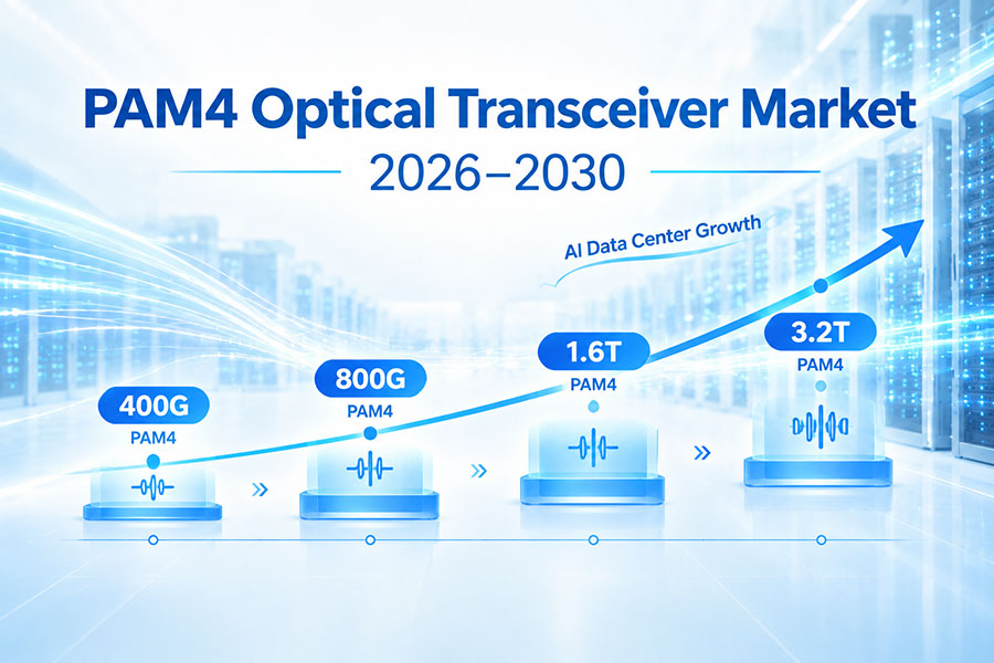
Silicon photonics is compatible with high-speed intensity-modulation formats such as PAM4. In a PAM4 system, four amplitude levels allow two bits to be carried per symbol.
By combining silicon photonic modulators with high-speed electrical interfaces, optical modules can support 50G-, 100G- and higher-rate optical lanes depending on the implementation.
The silicon photonic platform itself does not define the modulation format. PAM4, coherent modulation and other signaling approaches can use different photonic architectures.
7. Silicon Photonics vs Traditional Discrete Optics
| Feature | Silicon Photonics | Traditional Discrete Optical Design |
|---|---|---|
| Integration | High | Lower |
| Optical Components | Multiple functions can be integrated on a PIC | More functions may use separate devices |
| Footprint | Potentially smaller | Can require more package space |
| Lane Density | High | Depends on package architecture |
| Manufacturing Approach | Wafer-scale photonic integration | More component-level assembly |
| High-Speed Scaling | Supports highly integrated architectures | Can become more challenging as component count increases |
| Packaging | Requires advanced optical coupling and packaging | Uses more established discrete component packages |
8. Optical Integration and Component Reduction
One of silicon photonics' important contributions is the ability to integrate several optical functions into a single photonic platform.
Waveguides, modulators and photodetectors can be positioned very close to one another. This can reduce the number of discrete optical interfaces and create more compact optical engines.
Fewer optical interfaces can also simplify certain portions of the assembly, although precise fiber coupling and package alignment remain important challenges.
9. Power Efficiency for AI Networking
Power efficiency is becoming one of the most important considerations in AI infrastructure. Every additional watt consumed by optical and electrical interconnects contributes to the overall power and cooling requirements of the data center.
Silicon photonics can support power-efficient architectures by reducing optical path complexity and enabling optics to move closer to high-speed switching silicon.
Current industry developments are increasingly combining silicon photonics with CPO and NPO architectures specifically to address bandwidth-per-watt requirements in AI networks.
10. Silicon Photonics and CPO
Co-packaged optics places optical engines very close to the switch ASIC rather than relying entirely on front-panel pluggable transceivers.
Silicon photonics is well suited to CPO because a photonic integrated circuit can provide multiple optical lanes within a compact optical engine.
NVIDIA's current silicon photonics networking platform uses silicon-photonics-based CPO switches and positions the technology around higher bandwidth density, power efficiency and large-scale AI networking.
11. Silicon Photonics and NPO
Near-packaged optics, or NPO, provides an intermediate position between traditional pluggable optics and CPO. The optical engine is placed close to the ASIC but remains separated from the package.
This architecture can reduce the length of high-speed electrical connections while retaining more physical separation than a fully co-packaged design.
Silicon photonics can serve as the optical foundation for NPO because its integrated optical functions can be packaged into compact engines located near the switching device.
12. Silicon Photonics and Coherent Optics
Silicon photonics is not limited to direct-detect optical modules. It can also provide photonic building blocks for coherent optical systems.
Coherent architectures require optical modulation, detection and signal-routing functions that can be implemented using photonic integrated circuits together with external lasers and high-performance electronics.
This makes silicon photonics relevant to both data center optical interconnects and longer-reach coherent DCI systems.
13. External Lasers and Silicon Photonic Chips
A silicon photonic integrated circuit does not necessarily generate its own optical carrier. Many architectures use an external laser source that supplies continuous-wave optical power to the photonic chip.
This separation allows the photonic circuit and laser technology to be optimized independently. It can also support architectures such as CPO and NPO where laser placement, serviceability and thermal management are important.
Intel's current silicon photonics roadmap includes optical chiplet concepts designed to be co-packaged with CPUs, GPUs and other SoCs, while using external optical sources in the broader architecture.
14. Thermal Management and Cooling
AI switches and optical modules operate under increasingly high power densities. Silicon photonics can reduce some electrical interconnect challenges, but it does not eliminate thermal design requirements.
As optics move closer to ASICs, the optical engine operates in a thermally demanding environment. The laser, modulator, detector, driver and DSP must remain within their operating ranges.
This is why liquid cooling, improved heat spreading and advanced package design are becoming increasingly relevant to high-density AI optical systems.
15. Packaging Challenges
Silicon photonics provides high integration at the chip level, but packaging remains a major engineering challenge.
Optical fibers must be accurately aligned with tiny photonic structures, while electrical connections must support very high-speed signals. Mechanical tolerances, thermal expansion and optical coupling efficiency all influence package performance.
For CPO and NPO, these requirements become even more important because the optical engine is positioned much closer to high-power switching silicon.
16. Silicon Photonics for AI Scale-Up and Scale-Out
| AI Networking Layer | Silicon Photonics Role |
|---|---|
| Scale-Up | Can support very high-density optical connectivity close to compute or accelerator systems |
| Scale-Out | Supports high-bandwidth connections between servers, racks and network switches |
| Scale-Across | Can contribute to high-capacity optical links between distributed AI data centers |
| Chip-to-Chip | Provides an optical pathway for moving connectivity closer to compute silicon |
The technology requirements differ by layer. Shorter connections emphasize density and power efficiency, while longer links place greater emphasis on optical budget, dispersion and transport architecture.
17. Silicon Photonics and AI Data Center Network Scaling
As AI factories scale to larger numbers of accelerators, network bandwidth must grow without allowing optical interconnect power and thermal requirements to increase at the same rate.
Silicon photonics supports this scaling by integrating multiple optical functions and enabling optical engines to move closer to switching and computing silicon.
Current industry developments illustrate this direction. NVIDIA's silicon-photonics CPO roadmap targets large-scale AI Ethernet and InfiniBand networks, while Coherent is demonstrating silicon-photonics CPO and NPO architectures for high-density AI infrastructure.
18. Key Benefits and Limitations
| Aspect | Silicon Photonics |
|---|---|
| Bandwidth Density | Supports highly integrated multi-lane optical architectures |
| Power Efficiency | Can reduce electrical interconnect overhead in suitable architectures |
| Integration | Combines multiple optical functions on a photonic chip |
| Scalability | Suitable for high-speed and high-density optical systems |
| Packaging | Requires highly precise optical and electrical assembly |
| Thermal Design | Becomes challenging when optics are placed near high-power ASICs |
| Laser Integration | Often requires external laser sources or separate laser integration |
| Manufacturing | Benefits from semiconductor-style wafer processing but still requires advanced optical packaging |
19. Silicon Photonics for AI Data Centers: Summary
Silicon photonics is becoming an important optical integration technology for AI data centers because it can combine multiple photonic functions into compact, high-density architectures. This makes it relevant to the industry's transition toward 800G, 1.6T and higher-bandwidth optical connectivity.
Its importance extends beyond conventional pluggable transceivers. Silicon photonics can serve as the optical foundation for optical engines, NPO, CPO and selected coherent architectures, allowing optical connectivity to move closer to switch and compute silicon.
The main benefits include integration density, potential power-efficiency improvements, scalable optical lane architectures and shorter high-speed electrical paths. At the same time, optical coupling, thermal management, external laser integration, manufacturing yield and package reliability remain important engineering challenges.
For AI data centers, silicon photonics should therefore be viewed as part of a broader optical ecosystem that includes lasers, modulators, photodetectors, DSPs, fiber attach, advanced packaging, cooling and network architecture.
 >
>

 >
>
 >
>
 >
>
 >
>
 >
>
 >
>
 >
>