TEL:+86 132 6656 7067





1. What Is PAM4 DSP?
PAM4 DSP refers to digital signal processing techniques used to generate, condition, recover and interpret four-level pulse amplitude modulation signals. PAM4 represents two bits in each symbol by using four different signal amplitude levels.
Compared with NRZ, PAM4 carries more information per symbol at the same symbol rate. However, the amplitude spacing between adjacent levels is smaller under comparable signal-swing conditions. This makes PAM4 more sensitive to noise, channel distortion, inter-symbol interference and timing errors.
DSP helps compensate for these impairments so that the receiver can distinguish the transmitted symbols and recover the original data.
2. Why PAM4 Requires Advanced Signal Processing
In NRZ signaling, the receiver distinguishes between two signal states. PAM4 introduces four amplitude levels and three decision boundaries. The smaller spacing between adjacent levels leaves less margin for noise and distortion.
Several channel effects can reduce the separation between PAM4 levels:
Insertion loss: High-frequency signal components are attenuated as they travel through electrical channels and interconnects.
Inter-Symbol Interference (ISI): Energy from previous symbols spreads into subsequent symbol periods.
Jitter: Timing variation shifts the sampling position and can cause incorrect symbol decisions.
Noise: Electrical and optical noise can make adjacent amplitude levels harder to distinguish.
Nonlinearity: Transmitter and receiver components may distort the expected relationship between signal input and output.
Bandwidth limitation: Restricted channel bandwidth changes pulse shape and reduces eye opening.
These impairments can increase the pre-FEC bit error ratio. DSP techniques help improve the signal presented to the decision circuit, although their effectiveness depends on the channel and implementation.
3. Main Functions of a PAM4 DSP
A PAM4 DSP may perform several signal-processing tasks. The exact functions depend on whether the device is used in the transmitter, receiver or a combined transceiver architecture.
Signal Equalization
Compensates for channel frequency response and inter-symbol interference to improve signal separation.
Clock Recovery
Extracts timing information from the incoming signal to establish suitable sampling positions.
Symbol Detection
Determines which of the four PAM4 amplitude states was transmitted.
Signal Calibration
Compensates for selected circuit variations, including offset and gain errors.
Transmit Pre-Equalization
Shapes the transmitted electrical waveform to compensate for predictable channel impairments.
Data Recovery
Reconstructs the received data stream after signal processing and symbol decisions.
Not every PAM4 transceiver uses a DSP that performs all these functions internally. Some tasks may be handled by the host ASIC, SerDes, analog front-end or a separate retiming device.
4. PAM4 DSP Transmitter and Receiver Architecture
The transmitter and receiver use different processing stages. The transmitter prepares the electrical data for optical conversion, while the receiver processes the detected signal to recover the original information.
Transmitter Signal Path
The transmitter-side processing may include data mapping, pulse shaping, pre-emphasis and equalization. The resulting electrical waveform drives an optical transmitter, such as an EML-based or silicon-photonics modulator architecture. Some implementations use different combinations of digital and analog processing.
Receiver Signal Path
In an ADC-based receiver, the photodetector and TIA convert the optical signal into an electrical waveform. An ADC samples the waveform, after which digital processing performs equalization, timing recovery and data decisions.
Some receiver architectures use analog equalization or mixed-signal processing instead of a fully digital implementation. Therefore, the internal signal path should always be checked against the specific transceiver design.
5. Feed-Forward Equalization (FFE)
Feed-Forward Equalization is a linear filtering technique used to compensate for channel distortion and inter-symbol interference. It combines multiple weighted samples of the signal to produce an adjusted output.
In a digital receiver, an FFE can use samples from earlier and later positions around the current sampling point. The filter coefficients, commonly called taps, determine how much each sample contributes to the output.
FFE is useful for correcting linear channel effects such as frequency-dependent attenuation and pulse spreading.
Reduces selected forms of inter-symbol interference.
Improves eye opening under suitable channel conditions.
Can be implemented in the transmitter as pre-equalization or in the receiver as post-equalization.
Requires appropriate coefficient selection and adaptation for the target channel.
Increasing the number of taps can provide more flexibility, but it also increases processing complexity, power consumption and implementation requirements.
6. Decision Feedback Equalization (DFE)
Decision Feedback Equalization is a nonlinear equalization technique that uses previous symbol decisions to estimate and compensate for post-cursor inter-symbol interference.
Unlike a purely linear FFE, a DFE uses the receiver's earlier decisions to calculate an interference correction for the current symbol.
Its main characteristics include:
Can reduce post-cursor ISI that remains after linear equalization.
Uses previously detected symbols to estimate residual interference.
Can improve receiver performance in channels with significant post-cursor distortion.
May be vulnerable to error propagation when earlier symbol decisions are incorrect.
DFE design requires careful consideration of feedback timing, decision reliability and error behavior. Its use is implementation-dependent; not every PAM4 optical receiver uses the same DFE structure.
7. CTLE and Analog Front-End Equalization
Continuous-Time Linear Equalization (CTLE) is an analog equalization technique commonly used in high-speed electrical receivers. It adjusts the frequency response of the incoming signal, often increasing the relative contribution of higher-frequency components that have been attenuated by the channel.
CTLE is frequently used before digital processing to improve the signal presented to the ADC or decision circuit.
| Equalization Method | Processing Domain | Primary Function |
|---|---|---|
| CTLE | Analog | Adjusts frequency response to compensate for channel loss. |
| FFE | Analog or Digital | Uses weighted signal samples to reduce linear ISI. |
| DFE | Analog or Digital | Uses previous symbol decisions to compensate for post-cursor ISI. |
| Transmit Pre-Emphasis | Digital or Analog | Shapes the outgoing waveform to offset predictable channel loss. |
CTLE, FFE and DFE can be used in different combinations. The best architecture depends on channel characteristics, power constraints, latency requirements and receiver complexity.
8. Clock and Data Recovery (CDR)
Clock and Data Recovery extracts timing information from the received data stream. The receiver uses this timing reference to determine when to sample the signal and make symbol decisions.
Reliable clock recovery is especially important in PAM4 because timing errors can move the sampling point away from the center of an eye opening. When this occurs, the receiver may mistake one amplitude level for another.
CDR functions commonly include:
Detecting timing information from signal transitions.
Tracking frequency differences between transmitter and receiver clocks.
Adjusting sampling phase to reduce timing error.
Supporting stable symbol decisions under specified jitter conditions.
CDR can be implemented using analog, digital or mixed-signal techniques. Its location also varies: it may be integrated into a transceiver DSP, host SerDes or retiming device.
9. ADC and DAC in PAM4 DSP Architectures
Digital processing requires electrical signals to be represented in digital form. Analog-to-Digital Converters (ADCs) and Digital-to-Analog Converters (DACs) provide the conversion interfaces in many DSP-based transceiver designs.
| Component | Conversion Direction | Role in PAM4 Processing |
|---|---|---|
| ADC | Analog to Digital | Samples the received electrical waveform for digital signal processing. |
| DAC | Digital to Analog | Converts processed digital samples into an electrical waveform for the transmitter. |
ADC performance affects receiver resolution, sampling accuracy, bandwidth and power consumption. DAC performance affects transmitter waveform generation, linearity and signal quality.
Converter resolution alone does not determine overall transceiver performance. Sampling rate, effective number of bits, analog bandwidth, clock quality and circuit noise must also be considered.
10. PAM4 Symbol Detection and Decision Thresholds
After equalization and timing recovery, the receiver must determine which PAM4 symbol was transmitted. Four amplitude levels require three decision thresholds to divide the signal range into four decision regions.
In a simplified receiver, the measured signal amplitude is compared with these thresholds. The resulting symbol decision is then mapped back to its corresponding two-bit value according to the selected symbol mapping.
Real receivers must also account for noise, unequal level spacing, signal distortion and threshold variation. Calibration and adaptive processing can help maintain reliable decisions as operating conditions change.
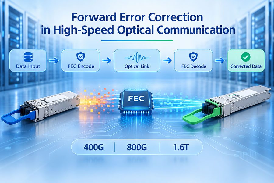
11. PAM4 DSP and Forward Error Correction
DSP and Forward Error Correction (FEC) work together in many high-speed PAM4 communication systems, but they perform different functions.
DSP improves the quality of the received signal and helps recover the transmitted symbols. FEC adds structured redundancy to the transmitted data so that the receiver can detect and correct a defined number of errors.
| Technology | Main Function | Primary Objective |
|---|---|---|
| DSP | Equalization, timing recovery and symbol detection. | Improve signal recovery before error correction. |
| FEC | Error detection and correction using redundant coding. | Correct errors within the code's correction capability. |
| BER Monitoring | Measures bit error performance. | Evaluate link quality before and after FEC. |
In many Ethernet implementations, FEC encoding and decoding are performed in the host or network-device PHY rather than inside the optical module's DSP. The exact allocation depends on the interface architecture and standard.
DSP cannot guarantee error-free transmission, and FEC cannot correct an unlimited number of errors. Both signal processing and coding performance must remain within the requirements of the applicable interface.
12. PAM4 DSP in 400G and 800G Optical Transceivers
High-speed Ethernet interfaces use PAM4 to increase the amount of information transmitted per symbol. DSP and related signal-conditioning functions help manage the electrical and optical impairments associated with these higher data rates.
| Network Speed | Illustrative Lane Configuration | Signal Processing Considerations |
|---|---|---|
| 400G | 4 × 100G or 8 × 50G | Lane equalization, timing recovery and PAM4 signal quality. |
| 800G | 8 × 100G | Higher aggregate bandwidth and tighter signal-integrity requirements. |
| 1.6T | 8 × 200G in relevant architectures | Higher lane rates, advanced electrical interfaces and more demanding channel design. |
These are illustrative configurations. Actual lane rates, optical mapping, DSP allocation and FEC requirements depend on the applicable Ethernet standard and product implementation.
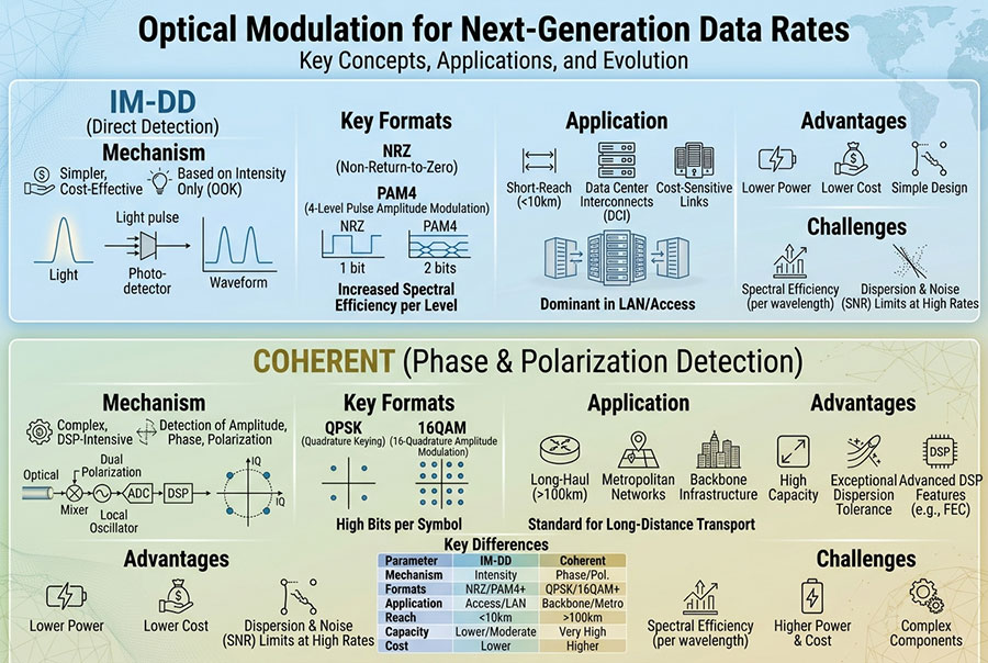
DSP architecture also differs between short-reach optical modules, longer-reach designs and coherent optical transceivers. A coherent DSP, for example, performs additional functions such as carrier recovery and compensation for chromatic dispersion and polarization effects.
13. DSP Power Consumption and Thermal Considerations
Signal processing improves link performance, but high-speed DSP circuits consume electrical power and generate heat. In compact optical modules, this creates a design trade-off between signal-processing capability, power efficiency and thermal performance.
Important design considerations include:
Processing complexity: More advanced equalization and signal recovery functions can increase circuit activity.
Converter power: High-speed ADCs and DACs can contribute significantly to the power budget.
Clocking requirements: High-speed timing and sampling circuits require careful power and noise management.
Thermal dissipation: Heat from DSP and analog circuits can affect module operating temperature.
Power efficiency: Processing architecture must meet performance targets without excessive energy consumption.
As optical modules move toward 800G and 1.6T, power efficiency and thermal design become increasingly important. These considerations influence module layout, heatsink design, host airflow and the selection of signal-processing architecture.
14. PAM4 DSP Testing and Performance Validation
DSP performance must be evaluated through electrical and optical measurements. Testing should verify that the complete signal path meets the relevant interface requirements under defined operating conditions.
| Test Item | What It Evaluates | Why It Matters |
|---|---|---|
| PAM4 Eye Diagram | Signal separation, eye opening and waveform quality. | Shows whether the four levels remain distinguishable. |
| Pre-FEC BER | Error performance before FEC correction. | Indicates the raw quality of the recovered data. |
| Post-FEC BER | Residual errors after FEC decoding. | Verifies corrected link performance. |
| TDECQ | Transmitter signal quality under the specified PAM4 measurement method. | Evaluates transmitter impairment and dispersion-related penalties. |
| Jitter Tolerance | Receiver ability to tolerate timing variations. | Checks clock recovery and sampling robustness. |
| Equalization Performance | Signal quality before and after equalization. | Shows how effectively channel impairments are compensated. |
| Power and Temperature | Module power consumption and thermal behavior. | Validates operation within platform limits. |
Testing should use the appropriate reference receiver, signal pattern, measurement bandwidth and test conditions for the target interface. A result from one PAM4 application should not automatically be treated as a pass/fail criterion for another.
15. Common PAM4 DSP-Related Link Problems
When a PAM4 optical link experiences unstable operation or elevated error rates, DSP-related factors should be considered alongside optical power, fiber quality and host compatibility.
| Observed Symptom | Possible Technical Cause | Relevant Investigation Area |
|---|---|---|
| High Pre-FEC BER | Insufficient signal margin, excessive ISI or noise. | Eye quality, equalization and channel loss. |
| Unstable Symbol Decisions | Timing error, poor level separation or threshold mismatch. | CDR, sampling phase and receiver calibration. |
| High TDECQ | Transmitter distortion, noise or waveform degradation. | Transmitter linearity and signal conditioning. |
| FEC Uncorrectable Errors | Raw error rate exceeds the correction capability. | Pre-FEC BER, optical margin and channel integrity. |
| Intermittent Link Operation | Host signal-integrity issues, configuration mismatch or environmental variation. | Host SerDes, module diagnostics and compatibility. |
DSP-related troubleshooting should not be limited to changing equalizer settings. Engineers should examine the complete electrical and optical channel, including host transmitter characteristics, module behavior, fiber connections and receiver performance.
16. PAM4 DSP and the Development of CPO
Co-Packaged Optics brings optical engines closer to the switch ASIC to reduce high-speed electrical interconnect distance and support higher bandwidth density. This changes where signal processing and optical conversion functions are located within the system.
Depending on the architecture, DSP and FEC functions may be distributed across the host ASIC, optical engine electronics and other system components. Retimed, linear-drive and co-packaged implementations can therefore have different signal-processing arrangements.
As CPO and other advanced optical architectures develop, designers must balance:
Electrical reach between the switch ASIC and optical engine.
Signal equalization and retiming requirements.
DSP power consumption and package thermal limits.
Optical engine performance and photonic integration density.
System-level FEC placement and interoperability.
Reducing or relocating DSP functions may lower power consumption and latency in some architectures, but it also places greater demands on electrical channel quality and analog circuit design.
17. C-LIGHT High-Speed Optical Connectivity Solutions
PAM4 signal processing supports the high-speed optical interfaces used in modern data centers and AI networks. Selecting an optical transceiver requires matching its data rate, form factor, optical reach, fiber type and host electrical interface to the target platform.
C-LIGHT Optical Transceiver Portfolio
High-speed optical connectivity options for data-center switches and compatible Ethernet platforms. Product configurations should be selected according to the required optical application and host interface.
400G optical connectivity for supported switching platforms, with product-family options for different reach and fiber deployment requirements.
High-bandwidth connectivity for data-center switching and next-generation Ethernet infrastructure.
High-speed optical solutions for AI networks, large-scale switching systems and advanced data-center interconnects.
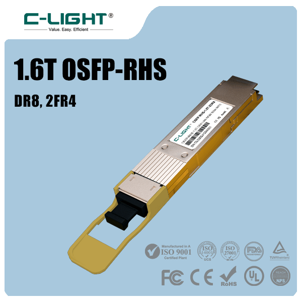
Next-generation optical connectivity for evolving high-capacity switching and data-center network architectures.
These are pluggable optical transceiver product families, not standalone DSP components. The DSP architecture, FEC allocation and supported signal-processing functions depend on each module design and its target interface specification.
18. Conclusion
PAM4 DSP is an important part of high-speed optical communication because it helps manage the signal-quality challenges associated with four-level modulation. Equalization, clock recovery, calibration and symbol detection work together to improve data recovery across demanding electrical and optical channels.
FFE, DFE and CTLE address different forms of signal distortion, while ADC and DAC circuits provide conversion between analog waveforms and digital processing. FEC complements these functions by correcting errors within its defined capability.
As 400G, 800G and 1.6T optical connectivity continues to develop, DSP architecture, power efficiency, thermal performance and signal-integrity testing will remain important factors in reliable optical transceiver design.
Explore High-Speed Optical Connectivity
C-LIGHT provides high-speed optical transceivers and connectivity solutions for data centers, AI networks and advanced Ethernet infrastructure. Contact our team for product specifications, compatibility support and project requirements.
Contact C-LIGHT >

 >
 >
 >
 >
 >
 >
 >