TEL:+86 132 6656 7067





Digital signal processing is a major contributor to power consumption in modern high-speed optical transceivers. As data rates advance from 400G to 800G and 1.6T, DSP architecture, signal processing complexity and thermal design increasingly influence module efficiency and system-level power requirements.
1. Why Optical DSP Power Consumption Matters
High-speed optical transceivers must process increasingly demanding electrical and optical signals while maintaining reliable transmission performance. In PAM4-based modules, the DSP compensates for channel impairments, supports signal recovery and helps maintain the required bit error rate across high-speed links.
These processing functions require substantial digital logic, high-speed SerDes interfaces, data converters and clock-related circuits. Their combined power consumption contributes directly to the module's electrical load and thermal output.
For a data center with thousands of optical ports, even a small reduction in power per module can produce meaningful savings in total electricity demand and cooling requirements.
2. How Much Power Does an Optical DSP Consume?
DSP power varies according to data rate, CMOS process technology, lane architecture, equalization requirements and the functions integrated into the chip. A higher-speed transceiver does not necessarily consume power in direct proportion to its bandwidth, because improvements in process nodes and circuit integration can offset part of the increase.
The figures above are broad reference ranges for selected module designs, not guaranteed values for every form factor or optical reach. Coherent modules, extended-reach products and high-temperature operating conditions can have substantially different power profiles.
| Module Generation | Typical Architecture | Representative Module Power | Main Design Consideration |
|---|---|---|---|
| 400G | 4 × 100G PAM4 optical lanes | About 8–12W | DSP processing and optical engine efficiency |
| 800G | 8 × 100G PAM4 optical lanes | About 13–18W | Higher lane count and thermal density |
| 1.6T | 8 × 200G or other high-speed lane configurations | Design-dependent; some designs around 20–30W | Advanced SerDes, DSP integration and cooling |
3. What Makes Up DSP Power Consumption?
An optical DSP is a complex signal-processing device rather than a single-purpose data converter. Its power consumption comes from several high-speed functional blocks operating together.
SerDes circuits transmit and receive high-speed electrical data between the host system and the optical module. High lane rates and demanding electrical channels increase their power requirements.
Analog-to-digital and digital-to-analog conversion support signal processing at the electrical and optical interfaces. Converter resolution, sampling rate and architecture affect power consumption.
CTLE, FFE and DFE compensate for frequency-dependent attenuation, inter-symbol interference and other channel impairments. More demanding equalization can require additional processing resources.
CDR circuits recover timing information from received signals. Their implementation and operating speed influence the power budget of the signal-processing subsystem.
Gearbox functions convert between different electrical and optical lane configurations when required. Integrated designs can reduce external components but still consume processing power.
Supporting logic handles configuration, diagnostics and operating-state management. Its contribution is usually smaller than that of the main high-speed processing blocks.
In many modern PAM4 modules, SerDes and data-conversion circuits are among the largest contributors to DSP power. The exact distribution depends on the chip architecture and the functions integrated into it.
4. Why DSP Power Increases at 800G and 1.6T
Higher data rates require more information to be processed within the same or a smaller physical footprint. Moving from 400G to 800G increases aggregate bandwidth and often increases the number of high-speed lanes. Moving toward 1.6T places even greater demands on electrical interfaces, signal integrity and thermal management.
PAM4 signaling carries two bits per symbol by using four signal levels. This improves bandwidth efficiency compared with NRZ, but the smaller separation between adjacent levels makes the signal more sensitive to noise, distortion and channel loss.
As symbol rates and lane speeds increase, the DSP must handle more demanding equalization, timing recovery and signal detection. Higher processing throughput can increase dynamic power, while more advanced CMOS processes and optimized circuit architectures help control the increase.
| Technical Factor | Impact on DSP | Power Implication |
|---|---|---|
| Higher lane rate | Increases processing throughput | Can increase SerDes and converter power |
| More electrical lanes | Requires more parallel signal paths | Increases aggregate circuit demand |
| Greater channel loss | Requires stronger signal compensation | May increase equalization complexity |
| Advanced FEC support | Adds coding and decoding functions where integrated | Depends on implementation and processing location |
| Advanced CMOS process | Enables more efficient high-density logic | Can reduce power per processing function |
5. DSP Power and the Total Optical Module Power Budget
A transceiver's power rating represents the consumption of the complete module, not just its DSP. The optical engine and supporting electronics also require power to generate, modulate, receive and monitor optical signals.
| Component | Primary Function | Power Characteristics |
|---|---|---|
| DSP | Signal processing, equalization and timing functions | Often a major power consumer in PAM4 modules |
| Laser Source | Generates the optical carrier | Depends on laser type and optical output requirements |
| Driver | Drives the optical transmitter | Depends on modulation method and drive requirements |
| TIA | Amplifies photodetector output | Depends on receiver bandwidth and sensitivity targets |
| TEC and Thermal Control | Controls component temperature where required | Can add significant power in temperature-controlled designs |
| Power Management | Converts and distributes internal supply rails | Includes conversion losses and control overhead |
The DSP share can exceed half of the total power in some high-speed module designs. However, the proportion changes with optical reach, laser technology, cooling requirements and DSP integration. A short-reach SR module and a long-reach or coherent module should not be assumed to have the same power distribution.
6. Thermal Management Challenges in High-Speed Optical Modules
Electrical power consumed by a transceiver is ultimately converted largely into heat. As module power increases, the available thermal margin becomes an important factor in maintaining stable operation.
Excessive operating temperature can affect laser characteristics, receiver performance, component reliability and the overall operating margin of the module. Thermal design therefore needs to consider both the DSP and the optical components rather than treating the DSP as an isolated heat source.
Key Thermal Design Considerations
Heat dissipation: The module housing and heat-transfer path must support the expected power level.
Airflow: Switch airflow, fan capacity and port density influence the temperature around optical cages.
Operating temperature: Power consumption and thermal behavior should be evaluated across the specified temperature range.
Port density: Fully populated switch panels can create concentrated heat loads.
System integration: Module cooling must be coordinated with switch ASIC, power supply and chassis thermal design.
In high-density 800G and 1.6T deployments, thermal performance is a system-level engineering requirement. A module that meets its individual power specification still needs to operate within the host platform's cooling and airflow limits.
7. Technologies That Reduce Optical DSP Power
Reducing DSP power is an important objective in next-generation optical interconnect design. Several approaches target different parts of the electrical and optical signal path.
Advanced CMOS Process Technology
Smaller semiconductor process nodes can improve logic density and reduce energy per operation when the chip is designed and optimized appropriately. Moving to a more advanced process does not guarantee a proportional reduction in total DSP power, because higher clock rates, additional processing functions and I/O requirements can offset some gains.
Silicon Photonics Integration
Silicon photonics integrates optical functions onto a photonic integrated circuit. It can reduce component count and improve optical integration, although the DSP and high-speed electrical interface may remain significant power consumers.
Linear Pluggable Optics
LPO reduces or removes the conventional retiming DSP from the optical module and relies more heavily on the host system's electrical signal processing. This can reduce module power and latency, but it places stricter requirements on host SerDes performance, electrical channel quality and system-level interoperability.
Linear Receive Optics
LRO uses a simplified optical module architecture, typically reducing some receiver-side signal-processing functions while retaining selected functions elsewhere. The actual power and latency benefits depend on the implementation and host platform.
Co-Packaged Optics
CPO places optical engines close to the switch ASIC, shortening high-speed electrical paths. This can reduce electrical channel loss and create opportunities for lower-power interfaces. Its overall benefits depend on optical engine design, packaging, serviceability and the complete system architecture.
| Technology | Power Reduction Approach | Main Engineering Consideration |
|---|---|---|
| Advanced CMOS DSP | Improves processing efficiency | Process, architecture and performance trade-offs |
| Silicon Photonics | Integrates optical functions | Optical integration and coupling efficiency |
| LPO | Reduces module-side DSP functions | Host signal integrity and interoperability |
| LRO | Simplifies selected receiver processing | Receiver architecture and host support |
| CPO | Shortens electrical paths to the optical engine | Packaging, cooling and serviceability |
8. What DSP Power Means for Data Center Operating Costs
Optical module power becomes increasingly important as data center bandwidth and port density grow. The energy used by transceivers contributes to both direct electrical consumption and the cooling load of the facility.
For example, if 1,000 optical modules each reduce their average power consumption by 2W, the direct reduction in module power is 2kW. If the modules operate continuously, this represents approximately 17,520 kWh of electricity over one year, before accounting for additional cooling-system effects.
This illustrates why small per-port improvements matter at scale. Network operators need to evaluate power consumption alongside link reach, bandwidth, reliability, compatibility and total cost of ownership.
9. Optical Transceiver Solutions for High-Speed Networks
Selecting an optical transceiver requires more than checking its nominal data rate. Module power, host compatibility, optical reach, connector type, operating temperature and thermal limits all influence deployment suitability.
400G QSFP-DD Optical Transceivers
Designed for high-bandwidth data center and network interconnect applications. The product family supports different optical configurations, with the exact power and reach depending on the selected model.
View 400G QSFP-DD Products →400G OSFP Optical Transceivers
An OSFP form-factor product family for high-speed switching and data center connectivity. Platform support, module power class and cooling requirements should be verified for each configuration.
View 400G OSFP Products →800G QSFP-DD Optical Transceivers
Built for next-generation high-density network infrastructure. Link reach, lane configuration and host-platform power support are important selection criteria.
View 800G QSFP-DD Products →800G OSFP Optical Transceivers
Designed for high-capacity data center interconnects and AI networking environments. Check the specific module's power consumption and thermal requirements before deployment.
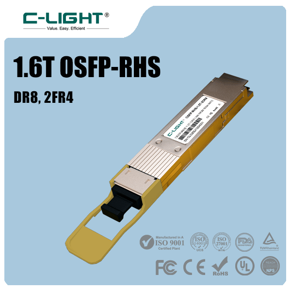
View 800G OSFP Products →1.6T OSFP-RHS Solutions
Intended for emerging 1.6T optical connectivity architectures. Host compatibility, cooling design, power delivery and optical configuration should be evaluated together.
View 1.6T OSFP-RHS Products →C-LIGHT provides optical connectivity solutions across multiple data rates and form factors. For a deployment requiring a specific power envelope, customers should confirm the exact module model, maximum power rating, operating temperature and host platform requirements before final selection.
10. Conclusion
Optical DSP power consumption is a major design consideration in high-speed PAM4 transceivers. As network bandwidth advances from 400G to 800G and 1.6T, higher lane rates, signal-processing complexity and thermal density place greater demands on module architecture.
Advanced CMOS processes, optical integration, LPO, LRO and CPO provide different paths toward improved energy efficiency. Each approach involves trade-offs in signal integrity, host compatibility, optical performance, serviceability and system design.
For data center operators, the most effective solution is not simply the module with the lowest DSP power. It is the transceiver and network architecture that delivers the required bandwidth, reach and reliability within the available power and cooling budget.
Planning a 400G, 800G or 1.6T Optical Network?
Contact C-LIGHT for optical transceiver product information and connectivity solutions for high-speed data center networks.
Contact C-LIGHT >

 >
 >
 >
 >
 >
 >
 >