TEL:+86 132 6656 7067





As data center networks move toward 400G, 800G, and 1.6T connectivity, conventional optical component architectures face increasing pressure from bandwidth density, power consumption, signal integrity, and thermal management. Silicon photonics (SiPh) addresses these challenges by integrating multiple optical functions onto a semiconductor photonic integrated circuit, creating a more compact and scalable foundation for high-speed optical communication.
By combining silicon-based waveguides, optical modulators, photodetectors, and other photonic components, silicon photonics can reduce the number of separately assembled optical elements. Its compatibility with semiconductor manufacturing processes also creates opportunities for wafer-scale production and more advanced optical packaging.
1. What Is Silicon Photonics?
Silicon photonics is a technology that uses silicon-based semiconductor platforms to guide, manipulate, and process light. Instead of building every optical function from an individual component, engineers integrate multiple photonic devices into a photonic integrated circuit (PIC).
A silicon photonic chip can contain optical waveguides, modulators, couplers, wavelength multiplexers, and photodetectors. These components work together to transmit and receive optical signals within a compact integrated structure.
Traditional optical integration
Individual optical components are assembled and connected through discrete optical paths, electrical connections, and mechanical structures.
Silicon photonic integration
Multiple optical functions are fabricated or integrated on a common photonic platform, reducing the need for separate optical components and complex internal connections.
Silicon photonics is not a complete replacement for every optical technology. It is an integration platform that combines silicon photonic devices with other semiconductor materials and electronic components where necessary.
2. How Does Silicon Photonics Work?
The core principle is to guide light through microscopic structures fabricated on a semiconductor chip. These structures control the movement and behavior of optical signals as they pass through the photonic circuit.
Key components of a silicon photonic chip
Optical waveguides
Waveguides confine and direct light across the photonic chip. Their geometry and refractive-index structure determine how optical signals propagate through the circuit.
Optical modulators
Modulators convert electrical data into optical signal variations. Mach–Zehnder modulators and electro-absorption modulators are important options in high-speed optical systems.
Photodetectors
Photodetectors convert incoming optical signals into electrical signals. Germanium-based photodetectors are commonly integrated with silicon photonic platforms.
Optical couplers and multiplexers
Couplers transfer light between fibers and waveguides. Multiplexers and demultiplexers combine or separate wavelength channels in WDM architectures.
How data moves through a silicon photonic transceiver
In a practical transceiver, electronic driver circuits, DSP functions, power management, and control circuits support the photonic components. The exact arrangement depends on the module architecture.
3. Why Silicon Photonics Improves High-Speed Optical Interconnects
The main advantage of silicon photonics is integration. By placing multiple optical functions on a compact chip, manufacturers can improve component density and create more scalable optical architectures.
Higher integration density
Traditional optical assemblies may require multiple discrete components, alignment operations, and internal connections. A photonic integrated circuit combines several functions on one platform, helping reduce component count and package footprint.
Potential for lower power consumption
Silicon photonics can support lower-power optical architectures through compact modulators, integrated optical paths, and closer integration between electronic and photonic circuits. Actual power consumption depends on the laser source, modulator, driver, DSP, coupling losses, and thermal design.
Scalable semiconductor manufacturing
Silicon photonics benefits from manufacturing infrastructure developed for the semiconductor industry. CMOS-compatible fabrication processes can support wafer-level production, repeatable device structures, and high-volume manufacturing.
Support for higher bandwidth density
Integrated waveguides and wavelength multiplexing allow multiple optical channels to occupy a compact photonic circuit. This is particularly valuable as data center switches and AI systems require more optical bandwidth within limited package and front-panel space.
| Design consideration | Discrete optical architecture | Silicon photonic integration |
|---|---|---|
| Optical components | Multiple separately assembled devices | Multiple functions integrated on a PIC |
| Package footprint | Depends on component count and assembly | Can reduce optical circuit footprint |
| Manufacturing approach | Component-level assembly and alignment | Semiconductor wafer processing plus packaging |
| Optical routing | Discrete optical paths and connections | On-chip waveguides and integrated routing |
| Scaling potential | Constrained by assembly complexity | Supports dense integration and multi-channel designs |
| Design challenges | Alignment, component count, and assembly | Coupling loss, thermal sensitivity, laser integration, and packaging |
These are architectural tendencies rather than universal performance guarantees. A well-designed discrete optical assembly may outperform a poorly optimized integrated design in particular applications.
4. The Role of Silicon Photonics in 400G, 800G, and 1.6T Transceivers
Higher network speeds require more optical bandwidth, more transmission lanes, or higher data rates per lane. Silicon photonics provides an integration platform that can support these developments through high-speed modulators, photodetectors, and wavelength multiplexing.
| Network generation | Typical bandwidth target | Design direction |
|---|---|---|
| 400G | 400 Gb/s | Multiple optical lanes using high-speed modulation and integrated photonic components |
| 800G | 800 Gb/s | Higher per-lane rates and denser optical integration |
| 1.6T | 1.6 Tb/s | 200G-class optical lanes, advanced modulators, and increasingly demanding packaging |
| Beyond 1.6T | Next-generation multi-terabit links | Higher lane rates, advanced materials, optical engines, and co-packaged architectures |
400G optical interconnects
Silicon photonics can integrate multiple optical functions into a compact transceiver design. Depending on the optical interface, a 400G module may use parallel optical lanes or wavelength-division multiplexing over fewer fiber connections.
For example, a four-wavelength architecture can combine multiple optical channels through an integrated multiplexer. This reduces the number of fiber strands required compared with an equivalent parallel optical arrangement, although the exact fiber configuration depends on the standard.
800G optical interconnects
At 800G, higher lane rates and increased optical integration become more important. Silicon photonic modulators and photodetectors can support compact optical engines, while integrated wavelength management helps address bandwidth density requirements.
Silicon photonics is one of the important technology platforms for 800G optical systems, but not every 800G transceiver uses the same photonic architecture. Module specifications, optical lane configuration, and component implementation vary by product.
1.6T and next-generation optical links
As 1.6T transceivers move toward wider deployment, optical components must support higher bandwidth per lane while maintaining acceptable power consumption, signal quality, and thermal performance.
Research into advanced silicon and germanium-silicon modulators, heterogeneous material integration, and high-speed photodetectors is helping extend the capabilities of silicon photonic platforms. These developments are important for future optical engines and next-generation data center interconnects.
5. Silicon Photonics and Co-Packaged Optics (CPO)
One of the most important applications of silicon photonics is co-packaged optics (CPO). Traditional pluggable transceivers are installed at the front panel of a switch, while the switch ASIC is located inside the equipment. High-speed electrical signals must travel between these two locations.
As interface speeds increase, long electrical connections can introduce greater signal loss and require more power for signal conditioning. CPO places optical engines much closer to the switch ASIC, shortening the high-speed electrical path.
Pluggable optical architecture
The optical transceiver is installed in a front-panel cage. Electrical signals travel between the switch ASIC and the module through the host board and connectors.
Co-packaged optical architecture
Optical engines are positioned close to the switch ASIC within the same package or package assembly, reducing the distance traveled by high-speed electrical signals.
Why silicon photonics is suitable for CPO
Compact optical engines: Integrated photonic circuits can provide multiple optical functions in a small footprint.
High bandwidth density: Multiple optical channels can be routed through a dense photonic structure.
Short electrical paths: Close integration with the ASIC can reduce electrical interconnect distance and associated signal-conditioning demands.
Flexible optical routing: Fiber arrays and optical connectors can carry high aggregate bandwidth away from the switch package.
However, CPO is not simply a silicon photonic chip placed next to a switch. It requires coordinated electrical design, optical packaging, fiber attachment, thermal management, testing, and field-service planning.
6. Silicon Photonics vs. Traditional InP-Based Optical Technology
Indium phosphide (InP) and silicon photonics are both important technologies in optical communications. They have different material properties and strengths, and they are often used together rather than as mutually exclusive alternatives.
| Technical aspect | Silicon photonics | InP photonics |
|---|---|---|
| Material platform | Silicon, often on silicon-on-insulator (SOI) | Indium phosphide semiconductor |
| Optical waveguides | Silicon waveguides with high index contrast | InP-based waveguide structures |
| Light generation | Usually requires an external or integrated non-silicon gain source | Can support integrated laser sources |
| Manufacturing foundation | Strong compatibility with CMOS-style fabrication | Specialized III-V semiconductor manufacturing |
| Integration strengths | Dense passive routing and integration of multiple optical functions | Active optical devices such as lasers and amplifiers |
| Key challenges | Laser integration, coupling, thermal sensitivity, and packaging | Manufacturing scale, cost, and integration complexity |
Why hybrid integration matters
Silicon has an indirect bandgap and is not an efficient material for conventional laser gain. Therefore, silicon photonic systems commonly use external laser sources or integrate III-V semiconductor materials with the silicon photonic platform.
In hybrid or heterogeneous integration, different materials are combined to use their respective strengths. Silicon can provide compact optical routing and integration, while III-V materials provide efficient light generation.
This approach is important for future optical engines because it avoids requiring one material platform to perform every optical function.
7. Technical Challenges of Silicon Photonics
Although silicon photonics offers significant integration advantages, high-speed deployment still depends on solving several device-level and system-level challenges.
Laser integration
Silicon does not efficiently generate laser light on its own. External laser sources or III-V material integration are therefore required. External laser arrangements can simplify thermal management, while integrated laser approaches may reduce some optical connections but introduce additional manufacturing and reliability considerations.
Optical coupling loss
Light must transfer between the photonic chip and external optical fibers. Edge couplers, grating couplers, fiber arrays, and precision alignment structures all affect coupling efficiency. In dense optical engines, even small coupling losses can influence the overall optical power budget.
Thermal sensitivity
Silicon photonic devices, particularly resonant structures such as microring resonators, can be sensitive to temperature changes. Thermal variations may shift optical operating wavelengths and require control or compensation.
High-speed modulation performance
As per-lane data rates increase, modulators must provide sufficient electro-optic bandwidth, low drive voltage, and acceptable signal quality. Material engineering and advanced modulator structures are being developed to extend performance beyond current generations.
Packaging and manufacturing yield
Photonic chips require accurate optical alignment and reliable electrical connections. Scaling production requires repeatable fiber attachment, wafer-level testing, advanced packaging, and quality control across the complete optical engine.
The performance of a silicon photonic chip does not determine the performance of the entire transceiver by itself. Laser characteristics, coupling efficiency, driver electronics, receiver design, DSP, FEC, packaging, and thermal conditions all contribute to the final system result.
8. How Silicon Photonics Affects Optical Interconnect Design
For data center architects and network engineers, silicon photonics changes more than the internal structure of an optical transceiver. It also influences how optical bandwidth is delivered, packaged, connected, and maintained.
Fiber infrastructure: Higher-density optical engines may require more organized fiber routing, high-density connectors, and carefully managed polarity.
Power planning: Engineers should evaluate the power consumption of the complete optical link, including lasers, DSP, drivers, and cooling.
Thermal architecture: Optical engines located near high-power ASICs require careful thermal isolation and cooling design.
Serviceability: Pluggable modules and CPO assemblies have different replacement and maintenance procedures.
Optical monitoring: Transmit power, receive power, temperature, and error statistics remain important for diagnosing link performance.
Platform compatibility: Optical interfaces, lane mapping, host electrical specifications, and firmware support must match the connected equipment.
9. C-LIGHT High-Speed Optical Interconnect Solutions
As network infrastructure evolves toward higher bandwidth, choosing the right optical transceiver and interconnect becomes increasingly important. The appropriate solution depends on the required data rate, transmission distance, fiber type, connector configuration, and host equipment.
High-Speed Optical Transceivers
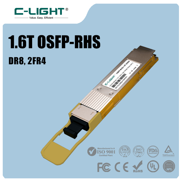
C-LIGHT provides optical transceiver solutions for data center and network applications. Available product categories include high-speed optical modules designed for different interface rates, form factors, and transmission requirements.
800G Interconnect Solutions
800G DAC – High-speed direct electrical connections for supported switch and server interfaces.
800G AOC – Active optical cable solutions for high-bandwidth connections.
800G AEC – Active electrical cable options for compatible high-speed platforms.
These cable assemblies serve different interconnect requirements and should be selected according to equipment compatibility, interface specifications, and link distance.
The products listed above are high-speed interconnect options, not a claim that every listed product uses a silicon photonic architecture. The underlying optical technology should be confirmed against the specific product datasheet.
10. Conclusion
Silicon photonics is an important technology for scaling high-speed optical interconnects. By integrating optical waveguides, modulators, photodetectors, and other photonic functions on semiconductor platforms, it supports higher integration density and more scalable optical engine designs.
Its role is becoming increasingly important in 400G and 800G networks, while 1.6T systems and co-packaged optics are driving further advances in modulator performance, laser integration, optical packaging, and thermal management.
Silicon photonics does not eliminate the need for other semiconductor materials or conventional optical components. Instead, its greatest value comes from combining photonic integration with suitable light sources, electronic circuits, packaging technologies, and fiber infrastructure to build more efficient high-bandwidth communication systems.
Contact C-LIGHT for optical transceiver and high-speed connectivity solutions tailored to your network requirements.
Contact C-LIGHT >

 >
 >
 >
 >
 >
 >
 >