TEL:+86 132 6656 7067





Optical engine evolution is reshaping the design of 800G and 1.6T transceivers through higher per-lane data rates, photonic integration, advanced packaging, and closer integration between optical and electronic components. These developments address the growing bandwidth, power-efficiency, signal-integrity, and thermal requirements of AI data centers and next-generation Ethernet networks.
1. What Is an Optical Engine?
An optical engine is the core assembly responsible for converting electrical data into optical signals and converting incoming light back into electrical signals. Depending on its architecture, it can contain a photonic integrated circuit (PIC), laser source or laser interface, optical modulators, photodetectors, wavelength multiplexers, and associated electronic components such as drivers and transimpedance amplifiers (TIAs).
Within a conventional pluggable transceiver, the optical engine operates alongside high-speed signal-processing circuitry, management electronics, power delivery, and thermal components. The complete module provides the electrical host interface, optical interface, and mechanical packaging required for connection to a switch or network device.
As network speeds increase, optical engines must support higher bandwidth within a limited physical footprint. The evolution from 400G to 800G and 1.6T therefore involves more than increasing the transmitter or receiver data rate. It requires coordinated improvements in photonics, electrical interfaces, packaging, signal processing, and manufacturing.
The optical engine is also becoming an important building block for linear pluggable optics (LPO), near-packaged optics (NPO), and co-packaged optics (CPO). These architectures change how closely the optical components are positioned to the host ASIC and how the electrical and optical functions are distributed across the system.
2. From Discrete Optical Components to Photonic Integration
Early high-speed optical designs relied heavily on separate optical components connected through individual electrical and optical interfaces. Although this approach offers flexibility in component selection, increasing channel counts can create challenges in assembly complexity, package size, electrical routing, and alignment.
Photonic integration combines selected optical functions on a shared photonic chip. Waveguides, modulators, photodetectors, and wavelength-selective structures can be integrated according to the chosen technology and manufacturing process. Electronic integrated circuits provide the high-speed electrical functions required to drive the transmitter and recover received signals.
The degree of integration varies significantly by design. Some architectures integrate much of the optical transmit and receive path into a PIC while retaining a separate laser source. Others use different levels of hybrid integration or combine photonic and electronic components within advanced packages.
| Architecture Stage | Typical Design Characteristics | Main Engineering Objective |
|---|---|---|
| Discrete optical assemblies | Separate optical components and electrical interfaces | Provide flexible component-level implementation and assembly |
| Integrated optical subassemblies | Multiple optical functions combined within a compact assembly | Reduce component count and simplify optical alignment |
| Photonic integrated circuits | Multiple optical functions integrated on a photonic chip | Increase optical integration density and support repeatable manufacturing |
| Advanced electronic-photonic packaging | PICs, electronic ICs, laser interfaces, and other components assembled within a coordinated package | Shorten critical electrical paths and improve bandwidth density |
| Near-packaged or co-packaged optical engines | Optical engines positioned near or alongside the host ASIC | Reduce the electrical distance between switching silicon and optical conversion |
Integration does not eliminate the need for precise optical design. Laser coupling, waveguide loss, thermal interaction, packaging tolerances, electrical parasitics, and manufacturing yield remain important. The objective is to improve overall system performance rather than maximize integration density in isolation.
3. Optical Engine Requirements at 800G
800G transceivers increase aggregate port bandwidth for high-capacity switching, AI cluster networking, and hyperscale data center infrastructure. Supporting this bandwidth requires an optical engine that can handle multiple high-speed channels while meeting the electrical, optical, power, and thermal requirements of the selected interface.
One representative architecture uses eight lanes operating at approximately 100Gbps per lane. Other implementations can use fewer lanes at higher per-lane rates, depending on the electrical interface, modulation format, optical physical layer, and system design.
The optical engine must preserve the required signal quality across the transmitter, optical path, and receiver. Its design commonly addresses several interconnected requirements:
High-speed modulation: Support the specified signaling rate and modulation format, including PAM4 where applicable.
Electrical-to-optical conversion: Maintain adequate transmitter bandwidth, optical output, and signal quality.
Optical channel integration: Combine or separate wavelengths where the architecture uses wavelength-division multiplexing.
Receiver performance: Provide suitable bandwidth, sensitivity, and error performance for the intended optical link.
Signal processing: Implement the DSP and FEC functions required by the selected physical layer, where applicable.
Thermal control: Maintain stable operation at the module's specified power and operating temperature.
At 800G, different optical engines may target short-reach multimode links, parallel single-mode fiber, wavelength-multiplexed links, or coherent transmission. These alternatives use different photonic structures and should be evaluated against their intended applications rather than treated as interchangeable designs.
4. The Transition to 1.6T and 200G-Class Lanes
The move to 1.6T increases the aggregate bandwidth available from a single transceiver or optical interface to approximately twice that of an 800G solution. One representative architecture uses eight 200G-class lanes, although actual electrical and optical implementations depend on the specified interface.
Higher per-lane rates place additional demands on photonic devices and electrical circuitry. Modulators, detectors, drivers, TIAs, package interconnects, and host channels must support the target bandwidth without introducing unacceptable noise, distortion, or signal loss.
| Design Factor | 800G Generation | 1.6T Generation |
|---|---|---|
| Aggregate bandwidth | Up to 800Gbps | Up to 1.6Tbps |
| Representative lane architecture | 8 × 100G-class lanes or selected higher-rate lane designs | 8 × 200G-class lanes in representative implementations |
| Signal integrity | High-speed channel loss, PAM4 quality where applicable, and lane consistency | Tighter channel margins, higher bandwidth requirements, and increased sensitivity to parasitics |
| Photonic integration | Multi-channel integration and compact optical packaging | Greater integration density and more demanding component and package design |
| Thermal design | Manage module power and heat at high port density | Address higher total throughput while maintaining platform-specific power and cooling limits |
| Validation emphasis | Lane performance, optical budget, DSP/FEC behavior, and compatibility | Per-lane signal quality, advanced packaging, thermal behavior, and complete system qualification |
These lane configurations are representative rather than universal. The electrical lane rate, optical lane rate, modulation format, number of wavelengths, and aggregate line rate do not always map one-to-one. The exact module specification determines how signals are distributed across electrical and optical channels.
For example, an optical interface may use parallel optical channels, while another module with the same aggregate bandwidth may use wavelength multiplexing. The optical engines must be engineered for the corresponding channel structure and fiber interface.
5. Silicon Photonics and EML-Based Optical Engines
Silicon photonics and electro-absorption modulated laser (EML) technology are two important approaches used in high-speed optical transmitters. They differ in how the light source, modulator, and supporting optical functions are implemented.
Silicon photonics
Silicon photonics uses photonic structures fabricated on a silicon-based platform to guide and manipulate light. Depending on the design, a silicon photonic integrated circuit can incorporate waveguides, modulators, wavelength multiplexers, and portions of the receiving path.
Silicon itself is not generally used as the light-generating source in conventional silicon-photonic transceivers. The architecture therefore needs a compatible laser source, which may be external, hybrid-integrated, or implemented through another supported integration approach.
The principal attraction of silicon photonics is the ability to integrate multiple optical functions with established semiconductor manufacturing processes. However, performance depends on the specific PIC design, coupling losses, laser arrangement, packaging, and manufacturing capability.
EML-based transmitters
An EML combines a laser and an electro-absorption modulator within a semiconductor device. The laser generates the optical carrier, while the modulator encodes electrical data onto the light.
EML technology can provide high-speed modulation and is used in various single-mode transceiver applications. Its advantages and limitations depend on the target data rate, wavelength, transmission distance, optical output requirements, and the integration of the EML with the rest of the engine.
| Characteristic | Silicon Photonics | EML-Based Transmitter |
|---|---|---|
| Photonic implementation | Uses integrated silicon-based waveguides and selected optical functions | Uses a laser and electro-absorption modulator integrated within a semiconductor device |
| Laser arrangement | Typically requires a separate or hybrid-integrated light source | Laser is integrated with the electro-absorption modulator |
| Integration approach | Supports integration of multiple photonic functions on a PIC | Combines laser and modulation functions in a compact optical source |
| Important design constraints | Coupling efficiency, modulator performance, laser interface, thermal tuning, and packaging | Modulation bandwidth, chirp, optical output, thermal behavior, and packaging |
| System-level assessment | Evaluate the complete PIC, light source, electronics, and optical assembly | Evaluate the EML together with the driver, receiver architecture, electronics, and thermal design |
Neither technology is universally superior. Selection depends on the desired optical performance, power budget, reach, manufacturing yield, cost targets, and the complete transceiver architecture.
6. Optical Engine Integration with DSP, Drivers, and TIAs
The optical engine cannot be assessed independently of its electronic interface. High-speed transmitters require driver circuitry to control the modulator or laser, while receivers use TIAs and subsequent circuitry to amplify and recover the electrical signal generated by the photodetector.
In DSP-based pluggable modules, the DSP compensates for selected electrical and signal-processing impairments and may implement functions required by the relevant interface. Its connection to the optical engine must preserve signal quality across the electrical channel.
Increasing the distance between the DSP or host ASIC and the optical components can make electrical transmission more challenging. Higher-frequency signals experience channel loss and may require additional signal conditioning, which can increase power consumption.
Optical engine evolution therefore focuses on the relationship between the optical and electronic functions. Advanced packaging can shorten sensitive electrical connections, improve interconnect density, and reduce some signal-integrity challenges. However, the overall result still depends on component performance, packaging parasitics, thermal behavior, and the chosen signal-processing architecture.
7. From DSP Pluggables to LPO, NPO, and CPO
Optical engine development is not limited to improving the components inside a conventional front-panel transceiver. It also involves deciding where the engine should sit relative to the switch ASIC and how much electronic signal conditioning should be used between the ASIC and the optical conversion point.
| Architecture | Optical Engine Location | Signal-Processing Approach | Primary Design Trade-Off |
|---|---|---|---|
| DSP-based pluggable optics | Inside a removable front-panel transceiver | Uses a DSP within the module for supported compensation and processing functions | Established modularity and serviceability, with power and electrical-channel constraints |
| Linear pluggable optics (LPO) | Inside a removable front-panel module | Reduces or removes the module's retiming DSP in the signal path for supported architectures | Potential power savings, with greater dependence on host and channel signal integrity |
| Near-packaged optics (NPO) | Mounted near the host ASIC on or close to the system board | Depends on the selected engine and system architecture | Shorter electrical connections while retaining a separable engine assembly |
| Co-packaged optics (CPO) | Integrated within the same package area as the host ASIC | Depends on the co-packaged electrical and photonic design | Very short electrical paths and high bandwidth density, with more complex system integration and serviceability |
DSP-based pluggable optical engines
DSP-based pluggable modules provide a removable optical interface with local signal-processing capability. This arrangement supports module replacement and familiar front-panel servicing, while the DSP helps manage electrical and signal impairments within the supported design.
Linear pluggable optics
LPO architectures reduce or eliminate selected retiming DSP functions inside the module, relying more heavily on the host transmitter, module analog front end, receiver, and electrical channel. Reducing DSP processing can lower module power in suitable implementations, but it places stricter demands on the host-to-module signal path and joint system qualification.
Near-packaged optics
NPO places optical engines closer to the host ASIC than a conventional front-panel module. Shorter electrical paths can improve the channel conditions and may reduce the need for some signal conditioning. Keeping the engine as a separate assembly can preserve a degree of modularity, although practical serviceability depends on the package, access, and replacement design.
Co-packaged optics
CPO integrates optical engines alongside the host ASIC within a shared package or tightly integrated package structure. Reducing the electrical distance between the ASIC and the optical engine can support higher bandwidth density and improve energy efficiency by reducing losses and signal-conditioning requirements on that path.
CPO also changes manufacturing and maintenance requirements. Optical engines, laser delivery, thermal management, fiber coupling, and package reliability become closely linked to the switching platform. Replacing a failed engine may be more complex than replacing a conventional pluggable module, depending on the implementation.
8. Thermal Management and Optical Engine Packaging
Higher data rates concentrate more functionality and signaling capability within a limited space. The photonic chip, laser source, driver, TIA, DSP, and associated power circuitry can produce localized heat, while the host switch ASIC and neighboring ports add to the total thermal load.
Temperature can affect laser wavelength, modulator behavior, analog circuit performance, component lifetime, and the stability of high-speed signal processing. Thermal design must therefore consider the optical engine and the complete host platform.
Heat dissipation in pluggable modules
High-density 800G and 1.6T modules require mechanical and thermal designs suitable for the host chassis. Heat sinks, cage geometry, airflow, electrical power delivery, and spacing between adjacent ports influence the module's operating conditions.
Reduced-height heat-sink designs, including OSFP-RHS implementations, target specific high-density system and cooling configurations. Their usefulness depends on compatibility with the host's mechanical arrangement and thermal interface rather than the package designation alone.
Cooling approaches for advanced optical systems
Conventional air cooling may be sufficient for some configurations, while higher-density systems may require improved airflow management, cold plates, or other liquid-cooling arrangements. The appropriate approach depends on the platform's thermal architecture and the power dissipated by its components.
For co-packaged systems, optical engines are closely associated with the host ASIC, making coordinated thermal engineering especially important. The design must maintain the required operating conditions for both electronic and photonic components while protecting optical alignment and package integrity.
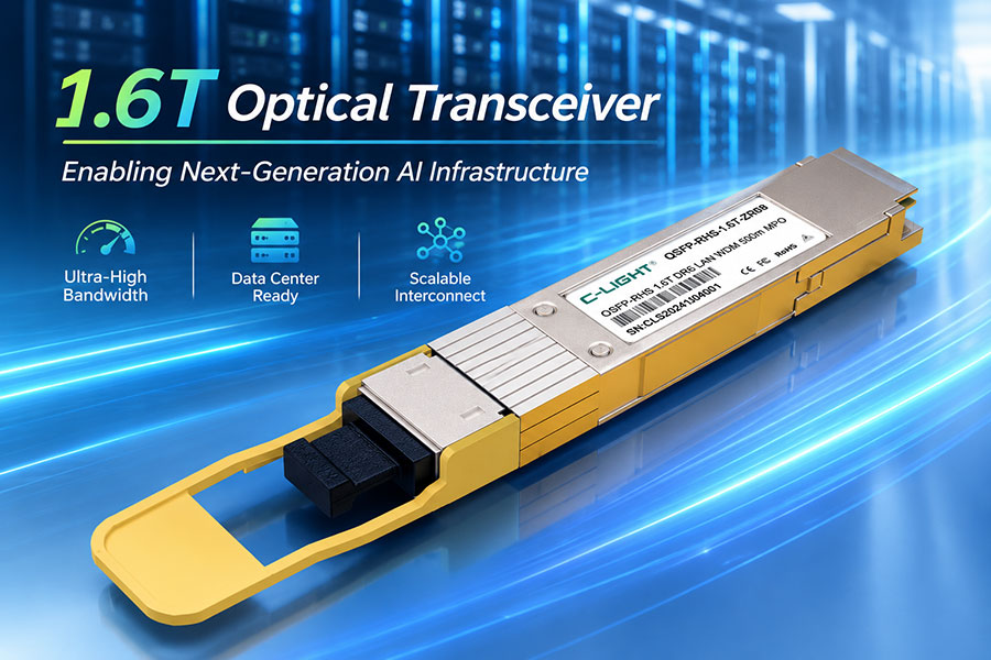
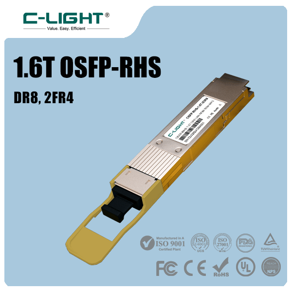
See the C-LIGHT 1.6T OSFP-RHS transceiver for an example of a high-density optical module designed around 200G-class lane signaling and a reduced-height heat-sink structure. Confirm the exact part number, optical interface, power requirements, and cooling conditions against the relevant datasheet.
9. Manufacturing, Optical Alignment, and Reliability
As optical engines become more integrated, the relationship between manufacturing precision and link performance becomes increasingly important. Small variations in optical coupling, component placement, electrical interconnects, or packaging can influence insertion loss, signal quality, and production yield.
Silicon photonics can integrate multiple optical functions on a chip, but the chip must still be coupled efficiently to its light source and the external fiber interface. EML-based and other optical architectures also require accurate placement, thermal control, and reliable electrical and optical connections.
Key engineering and manufacturing considerations include:
Optical coupling: Control alignment between the photonic chip, laser interface, and fiber assembly to meet the specified coupling-loss requirements.
Electrical interconnects: Minimize parasitic inductance, capacitance, and discontinuities that can degrade high-speed channel performance.
Thermal stability: Maintain suitable operating conditions across the PIC, laser source, electronic ICs, and package.
Assembly repeatability: Establish controlled manufacturing tolerances for component placement, optical attachment, and package assembly.
Production testing: Measure optical output, receiver performance, lane behavior, power, and management functions according to the product design.
Reliability qualification: Evaluate operation under the applicable environmental, temperature, vibration, and long-duration operating conditions.
Integration density does not guarantee higher production yield or easier repair. Performance depends on the design rules, process control, test coverage, packaging method, and maturity of the manufacturing process.
10. Optical Engine Validation for 800G and 1.6T
Testing should cover the individual engine and its behavior inside the complete transceiver or host system. Optical measurements alone cannot establish electrical signal integrity, and electrical compliance tests do not independently confirm optical reach or receiver performance.
| Validation Area | Test Focus | Purpose |
|---|---|---|
| Transmitter performance | Optical power, wavelength, modulation quality, and lane consistency | Confirms that the engine produces signals within the applicable specifications |
| Receiver performance | Receiver sensitivity, overload behavior where specified, and error performance | Verifies reception under defined optical input conditions |
| Electrical signal integrity | Channel loss, reflections, crosstalk, jitter, and signal quality | Checks the host-to-engine interface and internal high-speed electrical path |
| Lane-level performance | Individual channel status and error measurements where available | Identifies variations or faults that may be hidden by aggregate bandwidth readings |
| DSP and FEC behavior | Configuration, corrected and uncorrectable errors, and sustained link stability | Verifies the functions required by the selected physical-layer interface |
| Thermal performance | Module or package temperature, power consumption, and sustained operation | Ensures that operation remains within the platform's specified limits |
| Optical path validation | Fiber type, connector compatibility, insertion loss, and supported reach | Confirms compatibility between the engine and the intended optical link |
| System interoperability | Host port, firmware, module management, and end-to-end traffic | Verifies operation in the intended production system |
For 1.6T implementations with 200G-class lanes, validation should pay particular attention to the specified electrical and optical interface, lane mapping, packaging behavior, and per-lane error performance where accessible. The applicable test method depends on the module's actual architecture.
For NPO and CPO systems, testing must additionally reflect the integrated mechanical, electrical, optical, and thermal design. Fiber coupling, laser interfaces, package-level signal integrity, and maintainability can be as important as the performance of the photonic chip itself.
11. Choosing Optical Engine Technology for Different Deployments
The best optical engine architecture depends on the target link, host platform, port density, power limits, and operating environment. Decisions should be made at the system level rather than based only on a headline bandwidth or integration method.
| Deployment Requirement | Relevant Architecture Options | Primary Evaluation Criteria |
|---|---|---|
| Flexible field replacement | Conventional DSP-based pluggable transceivers | Module compatibility, serviceability, optical reach, and power consumption |
| Lower module power in a qualified platform | Suitable LPO implementations | Host signal quality, electrical channel length, interoperability, and system error performance |
| Shorter electrical path with a separate optical assembly | NPO | Board layout, packaging, optical access, thermal design, and replacement strategy |
| Maximum bandwidth density near switching silicon | CPO | Package integration, laser architecture, cooling, fiber attachment, and system reliability |
| Higher optical integration within a module | Silicon-photonic or other integrated optical engines | Photonic performance, light-source integration, packaging, manufacturing yield, and cost |
Pluggable optical engines continue to offer advantages in modularity and field replacement. LPO can reduce selected module processing and power requirements when the host channel supports it. NPO and CPO can shorten electrical paths, but introduce different packaging, thermal, and servicing considerations.
For most deployments, the appropriate selection requires a complete comparison of total power, optical reach, bandwidth density, reliability, manufacturing maturity, and system maintenance requirements.
12. Frequently Asked Questions
12.1 What is the main function of an optical engine?
An optical engine converts electrical data into optical signals and incoming optical signals back into electrical data. Depending on the architecture, it includes photonic components such as modulators and photodetectors, a laser interface, and associated electronic components such as drivers and TIAs.
12.2 Why is optical engine integration important for 800G and 1.6T?
Higher aggregate bandwidth requires more capable optical and electrical components within limited space and power budgets. Integration can increase functional density, simplify selected optical assemblies, and help reduce interconnect complexity, although manufacturing, coupling, and thermal challenges remain.
12.3 What is the difference between silicon photonics and EML technology?
Silicon photonics integrates selected optical functions on a silicon-based photonic chip and generally uses a separate or hybrid-integrated laser source. An EML integrates a laser and electro-absorption modulator within a semiconductor device. Both approaches can support high-speed optical transmission, depending on the implementation.
12.4 How does 200G per lane technology support 1.6T transceivers?
A representative eight-lane architecture using 200G-class signaling can provide an aggregate rate of 1.6Tbps. The exact optical and electrical lane mapping depends on the interface, modulation format, and module design.
12.5 How do LPO, NPO, and CPO differ?
LPO reduces selected signal-processing functions within a pluggable module. NPO places optical engines closer to the host ASIC while maintaining a separate engine assembly. CPO integrates optical engines alongside the host ASIC within a shared or tightly integrated package. Each approach has different power, signal-integrity, cooling, and maintenance trade-offs.
12.6 Does a more integrated optical engine always consume less power?
No. Integration can reduce some interconnect losses and signal-processing requirements, but total power also depends on the laser, photonic devices, electronic circuitry, cooling, and implementation. The complete system should be compared using equivalent bandwidth and operating conditions.
12.7 What should be tested before deploying an 800G or 1.6T optical module?
Verify the optical and electrical interfaces, optical reach, transmitter and receiver performance, signal integrity, lane consistency, management compatibility, power consumption, thermal behavior, and sustained error performance. Use the exact product specifications and host-platform requirements to establish acceptance criteria.
13. Summary
Optical engine evolution is enabling higher bandwidth and greater integration across 800G and 1.6T optical connectivity. Photonic integration, faster per-lane signaling, advanced electronic-photonic packaging, and improved thermal engineering are addressing the constraints that emerge as data center networks scale.
Silicon photonics and EML-based transmitters provide different implementation paths, while DSP-based pluggables, LPO, NPO, and CPO distribute optical and electronic functions in different ways. Each architecture involves trade-offs in signal processing, power consumption, bandwidth density, reliability, manufacturing, and serviceability.
Successful implementation depends on more than the optical engine itself. The laser source, receiver, electrical channel, packaging, fiber interface, host ASIC, cooling system, and validation process must operate as a coordinated design. This system-level approach is essential for reliable deployment of next-generation 800G and 1.6T networking infrastructure.
Evaluating 800G and 1.6T optical connectivity?
Review the 800G OSFP optical transceiver portfolio and 1.6T OSFP-RHS solutions for high-bandwidth data center and AI networking applications.
Contact C-LIGHTFor any questions, please contact us by email or WhatsApp.
Email: sales@c-light.com
WhatsApp: +86 132 6656 7067
 >

 >
 >
 >
 >
 >
 >
 >