TEL:+86 132 6656 7067





The continuous growth of AI computing, hyperscale data centers, and high-performance networking is pushing optical interconnect technology toward higher transmission rates per channel. While 100G-per-lane and 200G-per-lane architectures have become important stages in the development of high-speed optical modules, the industry is now working toward 400G per lane optical transmission.
400G per lane means that a single optical communication lane carries approximately 400 gigabits of data per second. Instead of increasing aggregate bandwidth mainly by adding more optical lanes, this approach raises the capacity of each individual lane. It could support future 3.2T optical interfaces using eight 400G lanes and create new possibilities for AI data center networks.
However, achieving 400Gbps on a single optical lane is considerably more challenging than increasing the total bandwidth of a transceiver. It requires higher-speed electrical signaling, advanced modulation, improved optical transmitters and receivers, sophisticated signal processing, and careful management of power and thermal performance.
1. What Does 400G Per Lane Mean?
400G per lane refers to an optical transmission architecture in which each individual optical lane carries a nominal data rate of 400Gbps.
In optical networking, the total bandwidth of a transceiver is determined by both the data rate of each lane and the number of lanes used. A simplified calculation is:
Aggregate bandwidth = Data rate per lane × Number of lanes
For example:
4 × 100G = 400G aggregate bandwidth.
8 × 100G = 800G aggregate bandwidth.
8 × 200G = 1.6T aggregate bandwidth.
8 × 400G = 3.2T aggregate bandwidth.
In this context, 400G per lane is not the same as a 400G optical transceiver. A conventional 400G module may combine several lower-speed optical lanes to achieve 400Gbps in total. A 400G-per-lane architecture places approximately 400Gbps on each individual optical channel.
This distinction is essential when discussing next-generation optical transmission technology.
2. 400G Per Lane vs 400G Total Bandwidth
The terms 400G optical transmission and 400G per lane optical transmission describe different things. The first normally refers to the aggregate capacity of a connection or transceiver. The second describes the capacity of one individual lane.
| Technology | Example Lane Configuration | Aggregate Bandwidth | Meaning |
|---|---|---|---|
| 400G optical transceiver | 4 × 100G | 400G | Four 100G optical lanes combined |
| 800G optical transceiver | 8 × 100G | 800G | Eight 100G optical lanes combined |
| 1.6T optical transceiver | 8 × 200G | 1.6T | Eight 200G optical lanes combined |
| 3.2T optical architecture | 8 × 400G | 3.2T | Eight 400G optical lanes combined |
These are representative bandwidth configurations rather than universal module specifications. Electrical lane counts and optical lane counts do not always match because a transceiver may use DSP, retiming, or gearbox functions to convert between host-side and line-side interfaces.
3. How Does 400G Per Lane Optical Transmission Work?
Increasing the data rate of one optical lane requires improvements across the entire transmission path. The host device first generates high-speed electrical signals. The optical transmitter converts these signals into modulated light, which travels through optical fiber. At the receiving end, a photodetector converts the optical signal back into an electrical signal for processing.
A simplified transmission path includes:
The switch ASIC or host device generates high-speed electrical data.
Electrical interface circuitry and DSP prepare the signal for transmission.
The optical driver controls the optical modulator or laser.
The optical transmitter converts the electrical signal into a modulated optical signal.
The optical signal travels through the fiber channel.
The receiver photodetector converts the incoming light into an electrical signal.
Receiver DSP and FEC processing help recover the transmitted data.
At 400Gbps per optical lane, every component must support substantially higher bandwidth than in previous generations. Signal integrity, noise, timing, optical power, and receiver sensitivity become increasingly important.
4. PAM4 Modulation and 400G Per Lane
PAM4, or four-level Pulse Amplitude Modulation, is a key modulation format for high-speed optical transmission. It uses four distinct signal amplitude levels to represent two bits per symbol.
Compared with NRZ, which uses two signal levels and carries one bit per symbol, PAM4 can transmit twice as many bits at the same symbol rate.
4.1 How PAM4 Represents Data
Each PAM4 symbol represents one of four possible signal levels:
| Signal Level | Bit Representation |
|---|---|
| Level 0 | 00 |
| Level 1 | 01 |
| Level 2 | 10 |
| Level 3 | 11 |
Because each symbol represents two bits, PAM4 increases the bit rate without requiring the symbol rate to increase by the same factor.
4.2 Why 400G Per Lane Requires Very High Baud Rates
For a simplified PAM4 calculation, each symbol carries two bits. A nominal 400Gbps lane therefore requires approximately 200 billion symbols per second, or 200GBaud, before accounting for encoding and forward error correction overhead.
In practical Ethernet signaling, the gross line rate is higher than the nominal payload rate because additional bits are required for coding and FEC. For example, an IEEE 400G-per-lane discussion uses a PAM4 signaling rate of approximately 212.5GBaud for a 425Gbps gross rate.
This is a major increase compared with established 100G-per-lane optical interfaces and the 200G-per-lane technology used in 1.6T architectures.
4.3 PAM4 Signal Quality Challenges
PAM4 provides higher data capacity, but it also creates more demanding signal-quality requirements.
Its four amplitude levels are closer together than the two levels used by NRZ. This reduces the voltage margin available for distinguishing adjacent symbols and makes the signal more sensitive to noise, distortion, and other impairments.
At 400G per lane, the transmitter, fiber channel, and receiver must maintain sufficient signal quality for reliable data recovery.
5. The Role of DSP and FEC
Digital Signal Processing (DSP) and Forward Error Correction (FEC) are important technologies for high-speed optical communication.
5.1 Digital Signal Processing
DSP performs signal-processing operations that help compensate for channel impairments and recover high-speed data.
Depending on the optical architecture, DSP functions may include:
Transmit and receive equalization.
Clock and data recovery support.
Signal conditioning and distortion compensation.
Lane alignment and timing management.
Digital compensation for channel impairments.
As the symbol rate increases, DSP implementation becomes more demanding. Processing bandwidth, power consumption, latency, and chip integration all require careful consideration.
5.2 Forward Error Correction
FEC adds redundant information to transmitted data so that certain errors can be detected and corrected at the receiver without requiring retransmission.
Higher-speed PAM4 signals are more sensitive to noise and distortion, making error correction an important part of reliable optical communication.
However, FEC is not a substitute for good optical design. Transmitter quality, receiver sensitivity, channel loss, and signal integrity must still remain within the required operating limits.
6. Optical Transmitter Technologies for 400G Per Lane
The optical transmitter is one of the most challenging parts of a 400G-per-lane system. It must generate a high-speed optical signal while maintaining sufficient bandwidth, linearity, and signal quality.
Several semiconductor and photonic technologies are being developed or evaluated for this purpose.
6.1 Electro-Absorption Modulated Lasers
Electro-Absorption Modulated Lasers (EMLs) combine a laser source with an electro-absorption modulator. The modulator controls the intensity of the emitted light according to the electrical data signal.
EML technology has been widely used in high-speed optical modules because of its performance characteristics in demanding transmission applications. Further improvements in bandwidth, modulation efficiency, and manufacturing processes are important for future lane-rate development.
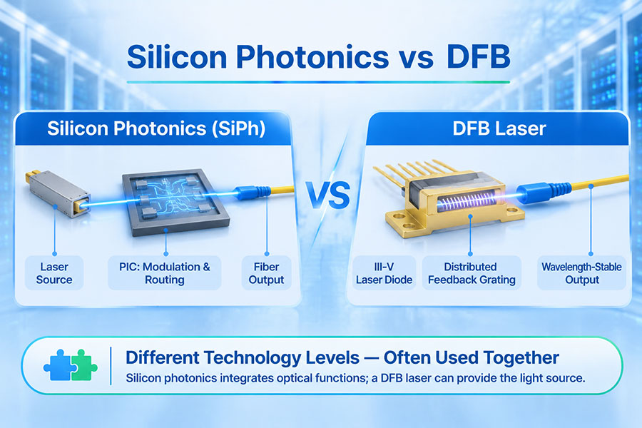
6.2 Silicon Photonics
Silicon photonics integrates optical functions onto silicon-based photonic circuits. It can support compact optical engines, wavelength management, and scalable integration with electronic components.
For 400G-per-lane applications, silicon photonics faces demanding requirements for modulator bandwidth, optical efficiency, signal linearity, and thermal stability.
Its potential advantages include integration density and the ability to combine multiple optical functions within a compact platform. The actual performance depends on the modulator design, material system, and overall optical architecture.
6.3 Thin-Film Lithium Niobate
Thin-film lithium niobate (TFLN) is another technology attracting attention for high-speed optical modulation. Its electro-optic properties make it suitable for developing modulators with very high bandwidth.
Research into TFLN modulators is relevant to future high-baud-rate optical transmission, although manufacturing scalability, integration, packaging, and commercial deployment remain important considerations.
7. Optical Receiver Challenges at 400G Per Lane
Increasing the transmitter data rate is only one part of the challenge. The receiver must also detect and recover the optical signal accurately at very high speeds.
Important receiver components include:
Photodetector: Converts incoming optical power into an electrical signal.
Transimpedance amplifier (TIA): Converts the photodetector's electrical current into a usable voltage signal.
Receiver DSP: Processes and equalizes the received signal.
Clock and data recovery: Helps identify the timing and data sequence of the incoming signal.
FEC decoder: Corrects supported transmission errors.
At 400G per lane, the photodetector and TIA must provide sufficient bandwidth while maintaining low noise and appropriate sensitivity. The receiver also needs to handle signal distortion introduced by the transmitter, optical fiber, and electrical interfaces.
8. Why 400G Per Lane Matters for 3.2T Optical Interconnects
One of the main reasons the industry is investigating 400G-per-lane technology is the demand for higher aggregate bandwidth without continually increasing the number of lanes.
Consider the following progression:
| Lane Rate | Number of Lanes | Aggregate Bandwidth |
|---|---|---|
| 100G | 8 | 800G |
| 200G | 8 | 1.6T |
| 400G | 8 | 3.2T |
With eight optical lanes, increasing the lane rate from 200G to 400G doubles the aggregate bandwidth from 1.6T to 3.2T.
This approach can increase bandwidth per module or optical engine while maintaining an eight-lane architecture. It is particularly relevant to future high-capacity switch interfaces and AI data center networks.
However, the move to 400G per lane requires a new generation of electrical interfaces, optical components, packaging, and signal-processing technology. It is not simply a matter of replacing an existing 200G optical module with a faster laser.
9. 400G Per Lane and AI Data Center Networks
AI data centers require high-bandwidth connections between GPUs, network adapters, switches, and other infrastructure. As cluster sizes and model complexity increase, network links must support larger volumes of east-west traffic.
400G-per-lane optical technology could help future AI networks scale their aggregate bandwidth while limiting the growth in lane count.
9.1 Higher Bandwidth per Optical Channel
Increasing the capacity of each optical lane can provide more bandwidth through a given number of optical channels. This can be useful in high-density network architectures where the number of physical ports, fibers, or optical engines is constrained.
9.2 Switch ASIC Bandwidth Scaling
Future switch ASICs need higher-speed electrical interfaces to connect to optical modules or optical engines. 400G-per-lane technology could support 3.2T-class optical interfaces and higher-capacity switch architectures.
9.3 Scale-Out Network Expansion
Large GPU clusters use scale-out networks to connect increasing numbers of compute nodes. Higher-capacity optical connections can support the bandwidth required between switching layers, although the complete network must be designed to avoid bottlenecks and excessive congestion.
The actual benefit depends on switch capacity, network topology, endpoint speeds, traffic patterns, and application behavior.
10. 400G Per Lane vs 200G Per Lane
200G-per-lane technology is an important foundation for 1.6T optical modules. Moving to 400G per lane represents another substantial increase in the transmission rate of an individual optical channel.
| Comparison Point | 200G Per Lane | 400G Per Lane |
|---|---|---|
| Nominal lane rate | 200Gbps | 400Gbps |
| Illustrative PAM4 baud rate | About 100GBaud | About 200GBaud |
| Eight-lane aggregate rate | 1.6Tbps | 3.2Tbps |
| Signal bandwidth requirement | High | Substantially higher |
| Optical component requirements | 200G-class transmitters and receivers | Next-generation high-bandwidth transmitters and receivers |
| Signal processing | Advanced DSP and FEC | More demanding DSP and FEC implementation |
| Development focus | 1.6T optical modules and networks | Future 3.2T optical interfaces and beyond |
The baud-rate figures are simplified PAM4 comparisons. Actual gross signaling rates depend on coding, FEC, and the interface specification.
11. What Are the Main Challenges of 400G Per Lane?
Although 400G per lane offers a path toward much higher optical bandwidth, several technical challenges must be addressed before it becomes practical across large-scale deployments.
11.1 Electrical Signal Integrity
At approximately 200GBaud-class PAM4 signaling, electrical channels must maintain very high bandwidth and low distortion. PCB traces, connectors, package transitions, and high-speed interfaces all affect signal quality.
11.2 Optical Modulator Bandwidth
The optical modulator must support the required symbol rate while maintaining suitable linearity and extinction performance. This places demanding requirements on the photonic material and modulator structure.
11.3 Receiver Sensitivity and Noise
Higher data rates reduce the time available to distinguish individual symbols. Receiver noise, bandwidth limitations, and optical impairments can therefore have a greater impact on data recovery.
11.4 Power Consumption
High-speed DSP, drivers, modulators, and receiver circuits can increase power requirements. For AI data centers with large numbers of optical connections, power per bit becomes an important design metric.
11.5 Thermal Management
Higher-performance optical engines and electronic components generate heat. Maintaining stable operating temperatures is essential for signal quality, reliability, and long-term operation.
11.6 Manufacturing and Cost
400G-per-lane components require precise manufacturing and packaging. Yield, test complexity, material selection, and production scalability will influence the cost and commercial availability of future optical solutions.
12. Is 400G Per Lane Already Used in Commercial Optical Transceivers?
400G-per-lane optical transmission is an emerging technology direction rather than a description of ordinary commercial 400G optical modules.
Commercially deployed 400G and 800G optical modules generally use multiple lower-rate optical lanes. The current 1.6T generation commonly uses 200G-class lanes, including eight-lane architectures.
400G-per-lane technology is being investigated for future high-capacity optical interfaces, including 3.2T-class architectures. Demonstrations and technology development do not mean that all corresponding transceiver standards, products, and deployment ecosystems are already commercially mature.
When evaluating a product, it is important to distinguish between:
Aggregate module bandwidth.
Electrical host lane rate.
Optical lane rate.
Symbol rate and modulation format.
Prototype or demonstration performance.
Commercial product specifications.
13. C-LIGHT and the Evolution Toward Higher Lane Rates
The transition toward 400G per lane is part of a broader evolution from 400G and 800G optical connectivity to 1.6T and future 3.2T network interfaces.
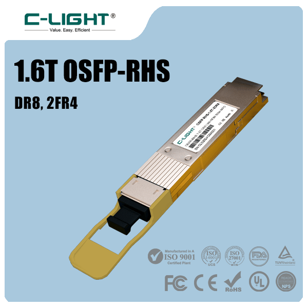
C-LIGHT's 1.6T OSFP-RHS optical transceiver represents the 200G-per-lane stage of this progression. Its eight-channel 200G PAM4 architecture provides an aggregate bandwidth of 1.6Tbps and is designed for AI data centers, GPU clusters, and high-density Ethernet networks.
The product portfolio includes 500m DR8 and 2km 2FR4 configurations, with different optical interface arrangements. These configurations should be selected according to the required transmission distance, host interface, and equipment compatibility.
For earlier network generations, C-LIGHT also offers 400G OSFP optical transceivers and 800G QSFP-DD optical transceivers. These products provide a practical reference for the existing multi-lane architectures that form the foundation for future higher-speed optical interfaces.
It is important to distinguish these current product generations from 400G-per-lane technology. The 1.6T OSFP-RHS uses 200G-class lanes; it is not a 400G-per-lane transceiver.
14. Conclusion
400G per lane optical transmission represents an important direction in the development of next-generation optical interconnects. By increasing the capacity of an individual optical channel to approximately 400Gbps, the technology could enable eight-lane 3.2T optical architectures and support the growing bandwidth requirements of AI data centers and hyperscale networks.
Reaching this performance requires more than a higher data rate. High-baud-rate PAM4 signaling, advanced optical modulators, high-bandwidth receivers, DSP, FEC, electrical signal integrity, and thermal management must work together.
Although 400G-per-lane technology is still an emerging development area, the progression from 100G to 200G and eventually 400G per lane illustrates how optical networking is evolving to support increasingly demanding compute and communication systems.
Frequently Asked Questions
Q1: What is 400G per lane optical transmission?
It is an optical transmission architecture in which one individual optical lane carries approximately 400Gbps, rather than combining multiple lower-speed lanes to achieve 400G total bandwidth.
Q2: Is 400G per lane the same as a 400G optical transceiver?
No. A conventional 400G transceiver can use multiple optical lanes. 400G per lane means that each individual optical channel carries approximately 400Gbps.
Q3: What modulation format is used for 400G per lane?
PAM4 is a major technology under consideration for 400G-per-lane optical transmission because it carries two bits per symbol.
Q4: What baud rate is required for 400G per lane?
A simplified PAM4 calculation gives approximately 200GBaud for 400Gbps. Actual gross signaling rates are higher when coding and FEC overhead are included.
Q5: How does 400G per lane enable 3.2T optical transmission?
An eight-lane architecture can provide 3.2Tbps by combining eight optical channels, each carrying 400Gbps.
Q6: What is the difference between 200G and 400G per lane?
400G per lane doubles the nominal capacity of a 200G lane. It also requires higher symbol rates, greater component bandwidth, and more demanding signal processing.
Q7: Why is DSP important for 400G per lane?
DSP helps compensate for signal impairments, manage timing, and recover high-speed data. Its performance is important for maintaining signal quality at very high baud rates.
Q8: What optical technologies may support 400G per lane?
Technologies being developed or evaluated include advanced EMLs, silicon photonics, and thin-film lithium niobate modulators. Their suitability depends on bandwidth, optical performance, integration, and manufacturing maturity.
Q9: Is 400G per lane commercially available in ordinary 400G optical modules?
No. Ordinary 400G optical modules generally combine multiple lower-rate optical lanes. 400G per lane is an emerging technology for future higher-capacity interfaces.
Q10: What is the relationship between 1.6T and 400G per lane?
A common 1.6T architecture uses eight 200G lanes. Increasing the lane rate to 400G in an eight-lane architecture would provide 3.2T aggregate bandwidth.
 >

 >
 >
 >
 >
 >
 >
 >