TEL:+86 132 6656 7067





Optical communication systems increasingly depend on electro-optic devices that can convert high-speed electrical signals into precisely controlled optical signals. As data center networks, coherent transmission systems, and AI infrastructure demand higher bandwidth, conventional modulator designs face growing pressure to improve modulation efficiency, electrical bandwidth, optical loss, and integration density. Thin-film lithium niobate (TFLN) has emerged as a promising photonic platform because it combines a strong electro-optic response with low optical propagation loss and a broad transparency window.
Unlike a complete optical transceiver, TFLN is primarily a material and device platform used to build photonic components. Its most important contribution to optical communication is the development of high-performance electro-optic modulators, although its potential also extends to optical switching, frequency conversion, and integrated photonic circuits.
1. What Is Thin-Film Lithium Niobate?
Thin-film lithium niobate is a photonic material platform based on a thin layer of lithium niobate (LiNbO₃) integrated onto an insulating substrate. It is commonly manufactured using lithium-niobate-on-insulator (LNOI) technology, in which a thin crystalline lithium niobate layer is bonded to an insulating layer and supporting substrate.
Bulk lithium niobate has been used for decades in optical modulators and other electro-optic devices. The thin-film approach changes the device geometry. By reducing the optical guiding layer to a submicrometer-scale structure, engineers can confine light more tightly and fabricate compact waveguides and photonic circuits.
Several material characteristics make lithium niobate particularly attractive:
Strong electro-optic effect: An applied electric field changes the material's refractive index, allowing electrical signals to control optical phase and intensity.
Low optical propagation loss: Carefully fabricated waveguides can support efficient optical transmission through integrated photonic circuits.
Broad optical transparency: Lithium niobate supports operation across a wide spectral range, depending on the waveguide and device design.
High-speed modulation potential: Traveling-wave electrode structures can support high-frequency electrical signals and broadband modulation.
Nonlinear optical properties: The material also supports nonlinear optical processes, including second-harmonic generation and other frequency-conversion functions.
These properties make TFLN useful for applications that require efficient control of optical signals without relying entirely on conventional carrier-based modulation mechanisms.
2. How Does the Electro-Optic Effect Work?
The central mechanism behind TFLN optical modulation is the Pockels effect, also known as the linear electro-optic effect. When an external electric field is applied to lithium niobate, its refractive index changes approximately in proportion to the applied field under the relevant operating conditions.
This change affects the phase of light traveling through the waveguide. By controlling the electric field, an electrical circuit can manipulate the optical phase and generate the modulation required to transmit digital information.
A simplified signal path is:
At the receiving end, a photodetector converts the optical signal back into an electrical signal. The receiver then processes the recovered data according to the communication system's architecture.
One widely used device structure is the Mach–Zehnder modulator (MZM). It splits incoming light into two optical paths, applies controlled phase changes to the light in each arm, and recombines the signals. The phase difference determines the output optical intensity.
Because lithium niobate has a strong electro-optic response, TFLN MZMs can achieve high-speed phase modulation while maintaining attractive optical performance. Device efficiency is commonly evaluated using parameters such as half-wave voltage (Vπ), interaction length, insertion loss, and electro-optic bandwidth.
3. Why Is TFLN Important for High-Speed Optical Modulation?
Optical communication speed depends on the complete transmitter and receiver architecture, not only the material used in the modulator. Nevertheless, the modulator is a critical component because it determines how effectively electrical data can be transferred onto an optical carrier.
TFLN offers several advantages for high-speed optical modulation:
Broad electro-optic bandwidth: Properly engineered traveling-wave electrodes can support high-frequency electrical signals.
Efficient phase modulation: The Pockels effect provides a direct mechanism for electrically controlling the optical phase.
Low optical loss potential: Low-loss waveguide fabrication helps reduce optical power loss within the photonic device.
Advanced modulation formats: TFLN modulators can support high-speed OOK and PAM-based transmission, as well as coherent modulation architectures.
Photonic integration: Multiple optical functions can be integrated into a compact photonic circuit.
These characteristics are particularly relevant as optical links move toward higher symbol rates and increasingly demanding signal formats. However, a high modulator bandwidth alone does not establish the achievable data rate of a complete optical link. Driver performance, receiver bandwidth, signal processing, fiber conditions, and forward error correction also influence system performance.
4. TFLN vs. Silicon Photonics vs. Indium Phosphide
TFLN is part of a broader ecosystem of photonic materials. Silicon photonics and indium phosphide (InP) are also widely used in optical communication, but each platform has different strengths and manufacturing considerations.
| Technology | Primary modulation mechanism or role | Key advantages | Main considerations |
|---|---|---|---|
| Thin-film lithium niobate | Linear electro-optic effect | Strong electro-optic response, low-loss waveguide potential, broad optical transparency | Fabrication, packaging, electrode design, and integration maturity |
| Silicon photonics | Commonly free-carrier plasma dispersion | Dense integration, semiconductor manufacturing ecosystem, compact photonic circuits | Carrier-related absorption, modulation efficiency, and thermal behavior |
| Indium phosphide | Electro-optic and carrier-based device structures | Active photonic functions, including lasers and optical amplifiers | Manufacturing cost, integration density, and process complexity |
| Bulk lithium niobate | Linear electro-optic effect | Established high-performance modulation technology | Larger device footprints and different integration characteristics |
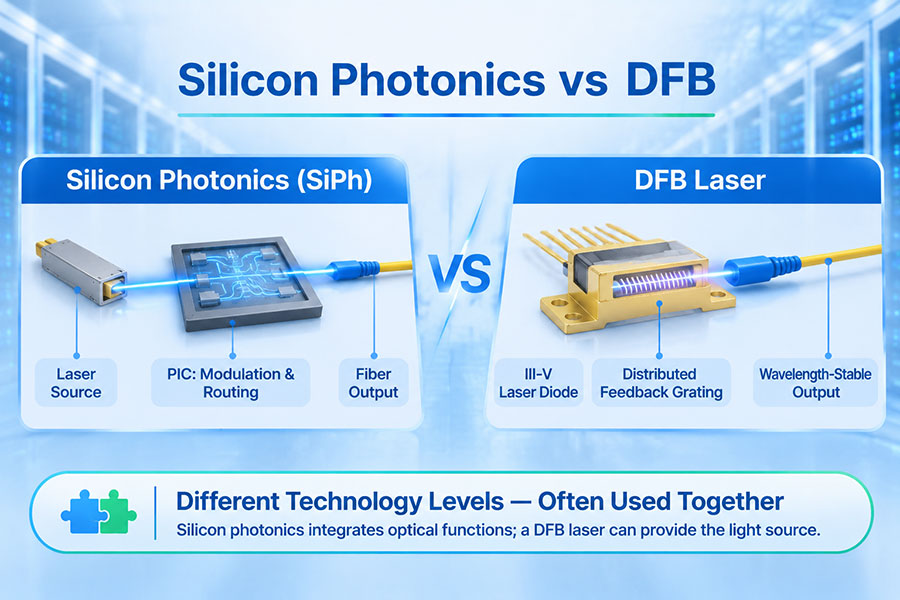
Silicon photonics has advantages in dense photonic integration and benefits from established semiconductor fabrication infrastructure. InP is especially important for active optical components, including semiconductor lasers and optical amplifiers. TFLN provides a strong electro-optic platform that can complement these technologies.
These platforms should not be treated as direct substitutes in every application. A photonic system may combine different materials to achieve the required modulation, light generation, amplification, detection, and routing functions.
5. The Role of TFLN in 400G, 800G, and 1.6T Optical Communication
As Ethernet and data center optical interfaces progress from 400G to 800G and 1.6T, transmitter components must support increasingly demanding electrical and optical signal requirements. High-speed modulators are one of the device technologies being developed to support this evolution.
TFLN is relevant because its electro-optic properties can support high-bandwidth modulation and integration into advanced optical engines. Research has demonstrated high-speed TFLN devices operating with PAM4 signals, a modulation format used in modern high-capacity optical communication systems.
However, it is important to distinguish between a modulator's laboratory transmission result and a commercially qualified transceiver. A complete 800G or 1.6T optical module also requires a suitable laser source, driver electronics, receiver components, DSP or other signal-processing functions where applicable, optical packaging, thermal management, and host electrical interfaces.
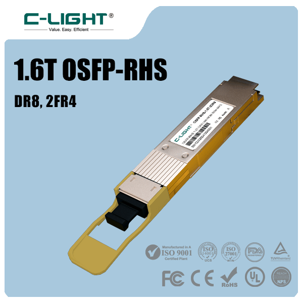
For current network deployment, C-LIGHT provides established product categories such as 400G QSFP-DD, 800G QSFP-DD, and 800G OSFP optical transceivers. These are complete connectivity products for supported network platforms. Their product specifications should be evaluated independently; the presence of a TFLN research ecosystem does not establish that a particular commercial module uses TFLN technology.
For 1.6T system development, TFLN may contribute to future optical engine designs where high modulation bandwidth, low optical loss, and compact integration are important. Actual implementation depends on the selected photonic architecture and product qualification.
6. TFLN in Coherent Optical Communication
Coherent optical communication uses both the amplitude and phase information of an optical carrier to transmit data. It enables high spectral efficiency and supports long-distance, high-capacity transmission when combined with suitable modulation formats and digital signal processing.
High-performance optical modulators are essential in coherent transmitters. Lithium niobate has a long history in this area because of its electro-optic properties. Thin-film implementations offer opportunities to reduce device size and improve photonic integration while retaining the material's modulation advantages.
TFLN can support coherent transmitter architectures that require precise phase and amplitude control. Depending on the design, integrated modulators can be used to generate advanced modulation formats such as QPSK and higher-order QAM signals.
Research has also demonstrated high-capacity coherent transmission using TFLN-based devices. These results highlight the material's potential for future coherent optical engines, although commercial performance depends on the complete transmitter, receiver, and transmission system.
7. Broadband Operation and New Optical Wavelengths
One of the distinctive properties of lithium niobate is its broad optical transparency. This creates opportunities for photonic devices that operate beyond a single conventional telecommunications wavelength band.
Most established fiber communication systems use the O-band and C-band, with other wavelength bands also relevant to specific network architectures. As demand for optical capacity grows, researchers are investigating additional usable spectral regions and multi-band transmission approaches.
A study published in Nature Communications in January 2026 demonstrated a TFLN electro-optic modulator with an operating range extending from approximately 1260 nm to 2060 nm. The reported device achieved more than 67 GHz of electro-optic bandwidth across the O-to-U bands, with approximately 100 GHz reported in several individual telecommunications bands. The researchers also demonstrated high-speed PAM4 transmission across multiple wavelength regions.
This is significant because a single broadband modulator platform could potentially support multiple optical bands. Nevertheless, a usable communication system also requires compatible lasers, photodetectors, optical amplifiers where needed, fiber transmission characteristics, and wavelength-specific components.
8. TFLN Beyond Modulators: Integrated Photonic Functions
Although electro-optic modulation is its most prominent optical communication application, TFLN can support several other photonic functions. Combining these functions on a common platform could help create more compact and flexible photonic integrated circuits.
Optical frequency conversion: Lithium niobate's nonlinear optical properties can support processes such as second-harmonic generation and difference-frequency generation.
Optical frequency combs: Electro-optic and nonlinear processes can generate multiple frequency components for applications involving wavelength channels and optical signal processing.
Optical switching: Electrically controlled refractive-index changes can support integrated optical routing and switching structures.
Phase control: Electro-optic phase shifters can control optical paths in interferometers and photonic circuits.
Microwave photonics: High-speed electro-optic devices can connect microwave and radio-frequency signals with optical processing and transmission systems.
These functions are relevant to future optical communication architectures because they may reduce the need for separate discrete components. However, integrating multiple functions on one chip requires careful management of optical loss, electrical routing, fabrication tolerances, and thermal behavior.
9. Technical Challenges Facing TFLN Commercialization
TFLN offers strong device-level advantages, but its commercial adoption depends on more than laboratory performance. Fabrication consistency, packaging, long-term stability, and production cost must all meet the requirements of communication equipment manufacturers and network operators.
Fabrication and integration: High-quality TFLN waveguides require precise patterning and etching. Sidewall roughness, material defects, and process variation can affect optical loss and device performance. Integration with electronic circuits and other photonic materials also requires carefully developed manufacturing processes.
Electrode design and RF performance: High-speed modulators use electrical electrodes to apply the modulation signal. Engineers must optimize impedance matching, microwave loss, and velocity matching between the electrical signal and the optical wave. These factors become increasingly important as operating bandwidth increases.
Bias stability: Mach–Zehnder modulators may require bias control to maintain the desired operating point. Temperature changes, material effects, and device-level drift can affect long-term stability. Practical products therefore need appropriate monitoring and control strategies.
Packaging and fiber coupling: A photonic chip must be connected reliably to optical fibers and electrical interfaces. Coupling loss, alignment tolerances, thermal expansion, and mechanical reliability all influence the performance of the packaged device.
Production economics: Wafer processing, photonic testing, packaging yield, and integration with other semiconductor technologies affect manufacturing cost. TFLN must demonstrate consistent performance at production scale to compete across high-volume optical communication markets.
10. What Recent Research Reveals About TFLN Development
Recent research shows that TFLN development is moving beyond the demonstration of basic electro-optic modulation. Researchers are improving bandwidth, modulation efficiency, optical loss, wavelength coverage, and integration density.
Several developments illustrate this progress:
Ultra-broadband modulation: A 2026 Nature Communications study reported a TFLN modulator operating across the O-to-U telecommunications bands and extending toward 2 μm, demonstrating high-speed PAM4 transmission in multiple spectral regions.
High-bandwidth device engineering: Research published in 2025 demonstrated a TFLN slow-light modulator with a measured electro-optic response up to 67 GHz, while its optimized electrode design showed a higher theoretical bandwidth potential.
Modulation efficiency: Research has investigated electrode and waveguide structures designed to improve the relationship between drive voltage, device length, optical loss, and bandwidth.
Integrated photonic circuits: Work on compact TFLN circuits is exploring multimode devices and denser integration for communication and photonic processing applications.
Long-term stability: Recent studies have examined bias drift mechanisms and methods for improving the operating stability of TFLN electro-optic modulators.
These developments indicate that the technology is advancing across both device performance and manufacturing-related challenges. The next important step is demonstrating repeatable, reliable, and cost-effective packaged devices that meet real network operating requirements.
11. The Future of TFLN in Optical Communication
The future role of TFLN will depend on how effectively its material advantages translate into complete optical communication products. Several application areas are particularly promising.
Next-generation data center optics: Higher-speed electrical and optical interfaces will require modulators with greater bandwidth and efficient signal conversion. TFLN is one candidate platform for future optical engines serving high-capacity data center links.
Coherent optical engines: Compact, high-performance modulators may support coherent transmission systems with higher bandwidth density and more integrated photonic functions.
Optical integration for AI infrastructure: As AI clusters increase the demand for high-bandwidth interconnects, integrated photonic devices will become increasingly important. TFLN could complement silicon photonics and other technologies in future optical engines, including selected near-packaged and co-packaged architectures.
Multi-band optical communication: Broadband TFLN devices may help support communication systems that use a wider range of optical wavelengths, subject to the availability of compatible fiber, sources, receivers, and network components.
Advanced photonic processing: The combination of electro-optic modulation, nonlinear optics, and integrated waveguides could enable more complex optical signal-processing functions on a common photonic platform.
It is unlikely that one material will dominate every part of the optical communication system. TFLN, silicon photonics, InP, and other photonic technologies are more likely to coexist, with each selected according to the requirements of the application.
12. Conclusion
Thin-film lithium niobate is an important development in integrated photonics because it combines a strong Pockels electro-optic effect, low-loss waveguide potential, broad optical transparency, and high-speed modulation capability. Its most immediate relevance to optical communication is in advanced modulators for high-capacity data center links, coherent optical systems, and next-generation photonic engines.
Research progress in broadband operation, high-speed PAM4 transmission, and integrated photonic circuits demonstrates the potential of TFLN. However, fabrication consistency, RF electrode performance, bias stability, packaging, and production cost remain important commercialization challenges.
Rather than replacing silicon photonics, InP, or existing optical transceiver architectures, TFLN is likely to become a complementary technology within a more diverse photonic ecosystem. Its long-term value will depend on how effectively it enables higher bandwidth, efficient modulation, and reliable integration in practical optical communication systems.
For current 400G, 800G, and other optical connectivity requirements, visit the C-LIGHT Optical Transceiver portfolio or Contact C-LIGHT for technical and product information.
 >

 >
 >
 >
 >
 >
 >
 >