TEL:+86 132 6656 7067





AI computing performance increasingly depends on how quickly processors, memory systems, and networking devices exchange data. Modern AI accelerators can execute enormous numbers of calculations, but their performance is also constrained by communication bandwidth, data movement, and the energy consumed by electrical interconnects. As accelerator clusters become larger, moving data between chips and systems is becoming an increasingly important part of overall computing architecture.
Photonic chiplets offer a potential solution by bringing optical communication functions closer to the processor package. Using silicon photonics and advanced packaging, these compact photonic devices can provide high-bandwidth connections between processors, switches, and distributed computing resources. Rather than replacing electronic computing, photonic chiplets extend the communication capabilities of AI hardware by moving data through optical channels where electrical connections become less efficient or practical.
1. What Are Photonic Chiplets?
Photonic chiplets are compact semiconductor components that integrate optical communication functions into a separate die or chiplet. They can be assembled alongside electronic processor dies, switch ASICs, or other components within an advanced package.
A photonic chiplet may contain several optical building blocks:
Optical modulators: Convert electrical data signals into modulated optical signals.
Photodetectors: Convert incoming optical signals back into electrical signals.
Optical waveguides: Guide light through the photonic integrated circuit.
Wavelength multiplexers and demultiplexers: Combine or separate multiple optical wavelengths to increase fiber capacity.
Optical couplers: Transfer light between the photonic chip and external optical fibers or other optical components.
Control and monitoring circuits: Support bias control, calibration, and operating-status monitoring, depending on the implementation.
The laser source may be integrated into the photonic chiplet, hybrid-bonded, or supplied by an external laser source. The architecture depends on the photonic platform, thermal requirements, and optical engine design.
Unlike a conventional standalone optical transceiver, a photonic chiplet is intended to participate directly in a larger semiconductor package or computing system. It provides an optical interface that can be integrated with the host processor or switch architecture.
2. Why Does AI Computing Need Photonic Chiplets?
Large AI models require extensive communication between processors, memory, and networking components. During distributed training and inference, accelerators exchange model parameters, gradients, intermediate results, and other data across high-speed interconnects.
As the number of accelerators increases, the communication network must support more aggregate bandwidth without consuming an excessive amount of power or package area.
Traditional electrical interconnects remain effective over short distances, but their performance becomes more difficult to scale as data rates and channel lengths increase. Electrical traces experience resistive losses, capacitive loading, crosstalk, and frequency-dependent signal distortion. Maintaining signal quality may require additional equalization, retiming, and power consumption.
Photonic chiplets address these limitations by converting electrical data into optical signals near the point where data enters the optical network.
The main motivations include:
Higher bandwidth density: Optical channels and wavelength multiplexing can support substantial aggregate data capacity through compact fiber interfaces.
Longer communication reach: Optical links can maintain high data rates over distances beyond practical high-speed electrical routing.
Lower electrical interconnect burden: Moving optical conversion closer to the processor can reduce the length of demanding high-speed electrical paths.
Improved system scalability: Optical connections can support communication between more processors, racks, and distributed computing resources.
Flexible network architecture: Optical links can connect computing resources through different physical layouts and network topologies.
3. How Do Photonic Chiplets Work in an AI Computing System?
A photonic chiplet provides an optical communication path between electronic computing components. The processor continues to perform digital computation, while the photonic chiplet handles the conversion and transmission of data through optical signals.
A simplified transmission process involves the following stages:
Data generation: The GPU, AI accelerator, or switch ASIC produces digital data for transmission.
Electrical interface: High-speed electrical signals travel from the host chip to the photonic chiplet through package-level connections.
Electrical-to-optical conversion: Optical modulators encode the data onto light generated by an integrated or external laser source.
Optical transmission: The modulated signal travels through optical waveguides, fiber arrays, or external optical fibers.
Optical reception: Photodetectors convert the incoming light into electrical signals at the receiving photonic interface.
Data processing: The receiving electronic chip processes the recovered data.
In a bidirectional architecture, each endpoint may include both transmitting and receiving functions. The physical implementation can use separate fibers, multiple wavelengths, or other optical channel arrangements.
The key benefit is that optical communication can extend high-bandwidth data movement beyond the limitations of dense electrical routing while allowing the processor to remain an electronic computing device.
4. Photonic Chiplets vs. Traditional Electrical Chiplets
Electrical chiplets and photonic chiplets perform different functions within advanced semiconductor packages. Electrical chiplets use conductive interconnects to transfer electrical signals, while photonic chiplets provide optical interfaces for data transmission.
| Feature | Electrical Chiplets | Photonic Chiplets |
|---|---|---|
| Signal transmission | Electrical signals through package traces and die-to-die connections | Optical signals through waveguides and fiber connections |
| Primary function | Logic, processing, memory, and electrical communication | Optical data transmission and electrical-to-optical conversion |
| Short-distance efficiency | Highly effective for short package-level connections | Requires optical conversion and additional photonic components |
| Longer-distance communication | Signal loss and power requirements become more challenging as distance increases | Optical transmission supports high-speed communication over longer distances |
| Integration requirements | Electrical routing, power delivery, and signal integrity | Electrical routing, optical coupling, laser supply, and thermal management |
| Major challenges | Electrical loss, crosstalk, routing density, and retiming power | Optical alignment, conversion efficiency, fiber attachment, and manufacturing yield |
| Typical applications | CPU, GPU, HBM, and processor die-to-die connections | Optical I/O, CPO, processor-to-processor links, and data center interconnects |
These technologies are complementary. Electrical chiplets remain important for tightly integrated logic and memory connections, while photonic chiplets can extend communication beyond the distances and bandwidth densities that are practical for electrical routing.
5. Photonic Chiplets and Advanced Packaging
Advanced packaging is essential because photonic chiplets must operate alongside electronic dies while maintaining precise optical and electrical interfaces. The package must support high-speed electrical connections, efficient optical coupling, thermal control, and mechanical reliability.
Several packaging approaches are relevant:
2.5D integration: Multiple dies are mounted on a common interposer or advanced package substrate. The interposer provides dense electrical connections between the electronic and photonic components. Depending on the architecture, it may also support optical routing or fiber interfaces.
3D integration: Electronic and photonic components can be arranged vertically using advanced stacking and bonding technologies. This can reduce interconnect distance and increase integration density, although thermal and manufacturing challenges become more complex.
Hybrid bonding: Fine-pitch bonding techniques can create dense electrical and mechanical connections between semiconductor components. They may support compact integration of photonic and electronic dies.
Fiber array attachment: Multiple optical fibers must be aligned with the photonic chip's optical interfaces. Precise alignment and stable mechanical attachment are essential for controlling coupling loss.
Thermal management: Photonic devices and electronic processors can have different temperature requirements. Package design must manage heat from the ASIC while maintaining stable optical performance.
The most suitable packaging architecture depends on the number of optical channels, data rate, optical interface location, cooling strategy, and manufacturing process.
6. Photonic Chiplets, Optical I/O, NPO, and CPO
Photonic chiplets are closely related to several emerging optical interconnect architectures, but the terms describe different parts of the system.
| Technology | What It Describes | Relationship to Photonic Chiplets |
|---|---|---|
| Photonic chiplet | A separate die containing optical communication functions | The photonic component that can be integrated into a larger package |
| Optical I/O | An optical input/output interface for transferring data between computing components | Photonic chiplets can implement the optical I/O interface |
| NPO | Near-packaged optics, where optical engines are placed near the main ASIC package | Photonic chiplets can form part of the optical engine |
| CPO | Co-packaged optics, integrating optical engines within or very close to the ASIC package | Photonic chiplets can provide the optical functionality in the package |
| Pluggable optics | Removable optical modules installed in front-panel ports | Different packaging architecture, although both use photonic integrated circuits |
In a CPO system, the photonic chiplet may be placed close to the switch ASIC to reduce the electrical distance between the two. In an optical I/O architecture, the photonic chiplet provides the interface that converts data between electrical and optical domains.
Photonic chiplets can also support processor-to-processor communication, optical memory expansion, and connections between computing packages. Their potential application is therefore broader than switch-based CPO alone.
7. The Role of Photonic Chiplets in GPU and AI Accelerator Networks
AI computing systems commonly use multiple accelerators working together to train or execute large models. These processors exchange data through high-bandwidth communication networks that can operate within a server, across racks, or between data center systems.
Photonic chiplets could support these networks at several levels.
Processor-to-processor communication: Optical interfaces can provide additional bandwidth between computing packages when electrical connections become difficult to scale.
Accelerator-to-switch connectivity: Photonic chiplets can support high-density optical links between AI accelerators and switching devices, helping move data across larger accelerator clusters.
Memory disaggregation: Optical interconnects can support communication with remote memory resources, allowing system designers to explore more flexible memory architectures. However, optical connectivity alone does not remove memory-controller, protocol, or latency constraints.
Scale-up networks: Optical links may extend high-bandwidth communication between processors or accelerators within a tightly connected computing system.
Scale-out networks: Photonic interfaces can support communication between servers and racks across larger AI clusters.
The potential value is not limited to increasing raw transmission speed. Photonic chiplets may also help system architects change how processors, memory, and networking resources are physically distributed.
8. Current Industry Progress and Technology Demonstrations
Photonic chiplets have progressed beyond purely conceptual architectures. Research institutions and technology companies have demonstrated optical I/O devices integrated with electronic processors and are developing packaging approaches for larger AI systems.
Several developments illustrate the direction of the industry.
Intel optical compute interconnect chiplet: In June 2024, Intel demonstrated an optical compute interconnect chiplet co-packaged with a CPU and operating with live data. The demonstration supported 64 channels at 32 Gbps in each direction and optical transmission over fiber distances up to 100 meters. It provided an example of how silicon photonics can be integrated into computing packages.
Photonic Fabric chiplet architecture: A 2026 IEEE ECTC conference paper presented a photonic chiplet approach for CPO in AI data centers. The architecture discussed assembly on organic substrates or interposers using die-to-die interfaces, including UCIe-related approaches. It also addressed signal integrity and thermal crosstalk considerations.
High-density optical chiplet development: In March 2026, Lightmatter announced sampling of its Passage CPO chiplet and reported a demonstration of 1.6 Tbps per fiber using a 16-wavelength DWDM architecture. This is a company-reported product milestone, not a universal performance specification for photonic chiplets.
Research on CPO for AI computing: A review published in Nature Electronics in August 2026 examined optical chip-to-chip interconnects and CPO architectures for high-performance computing and AI. It discussed 2D integration, 2.5D interposers, and 3D heterogeneous stacking, highlighting thermal management, manufacturability, and standardization as major development challenges.
These developments show growing interest in photonic chiplets as part of future AI infrastructure. However, demonstrations, sampled products, and large-scale commercial deployment represent different stages of technology maturity.
9. Technical Challenges Facing Photonic Chiplets
Despite their potential, photonic chiplets introduce several technical challenges that must be addressed before they can become widely adopted across AI computing platforms.
Optical coupling and alignment: The photonic chip must connect efficiently to external fibers or other optical components. Small alignment errors can increase insertion loss and reduce the available optical power margin.
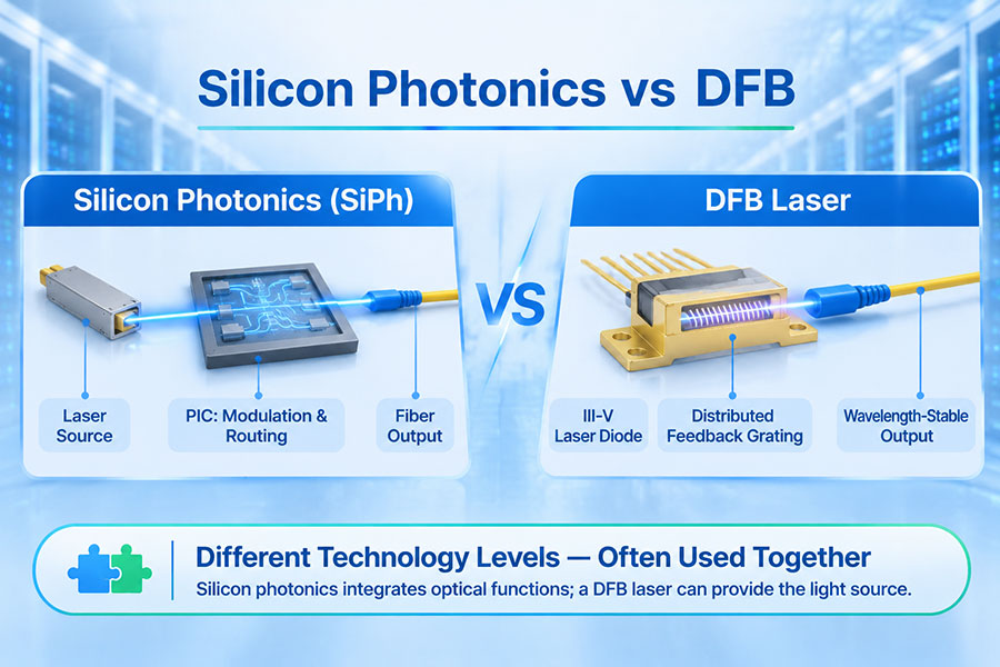
Laser integration: Silicon photonics does not generally provide efficient native light generation. Systems therefore need an appropriate laser solution, such as hybrid integration, heterogeneous integration, or external laser sources.
Thermal management: AI processors generate substantial heat. Temperature changes can affect laser wavelength, modulator characteristics, and photonic-device performance. Optical components require careful thermal design within the package.
Electrical-to-optical conversion: Drivers, modulators, photodetectors, and receiver electronics must operate together at the required data rate while controlling power consumption and signal degradation.
Manufacturing yield: Photonic chiplets combine optical and electronic interfaces that require different manufacturing and testing methods. A defect in one connection can affect the performance of the complete assembly.
Testing and repairability: Photonic devices require optical testing in addition to conventional electrical testing. Once multiple chiplets are integrated into a package, identifying and replacing a defective optical component can become more difficult.
Interoperability: Different photonic chiplets must work with compatible electrical interfaces, optical wavelengths, fiber connections, management systems, and package specifications.
Addressing these issues requires close cooperation between photonic-device designers, semiconductor foundries, packaging manufacturers, system architects, and optical networking suppliers.
10. Photonic Chiplets and the Future of 800G, 1.6T, and Beyond
As AI systems increase their aggregate communication requirements, optical interconnect capacity must scale alongside processor performance. 800G and 1.6T optical connectivity provide important reference points for the evolution of data center networks, while future optical I/O architectures may move beyond conventional front-panel module designs.
Photonic chiplets can contribute to this transition by placing optical communication functions closer to the computing package. Their development is associated with several important directions:
Higher-speed electrical interfaces: Faster SerDes and die-to-die connections are needed to connect electronic processors to photonic chiplets.
More optical wavelengths: WDM can increase aggregate bandwidth without requiring a proportional increase in fiber count.
Higher bandwidth per fiber: Improved modulation, multiplexing, and optical-engine integration can increase data capacity through each optical connection.
Advanced 2.5D and 3D packaging: More compact integration can reduce electrical path length and increase optical channel density.
External laser architectures: Separating laser generation from the photonic package can support thermal isolation and independent source maintenance.
Optical memory and processor connectivity: Optical I/O may support future systems that distribute computing and memory resources across larger physical distances.
For current network infrastructure, conventional pluggable optical transceivers remain important. C-LIGHT provides high-speed optical connectivity products including:
400G QSFP-DD Optical Transceivers for supported 400G network platforms.
400G OSFP Optical Transceivers for compatible OSFP equipment.
800G QSFP-DD Optical Transceivers for high-bandwidth data center connectivity.
800G OSFP Optical Transceivers for compatible 800G optical systems.
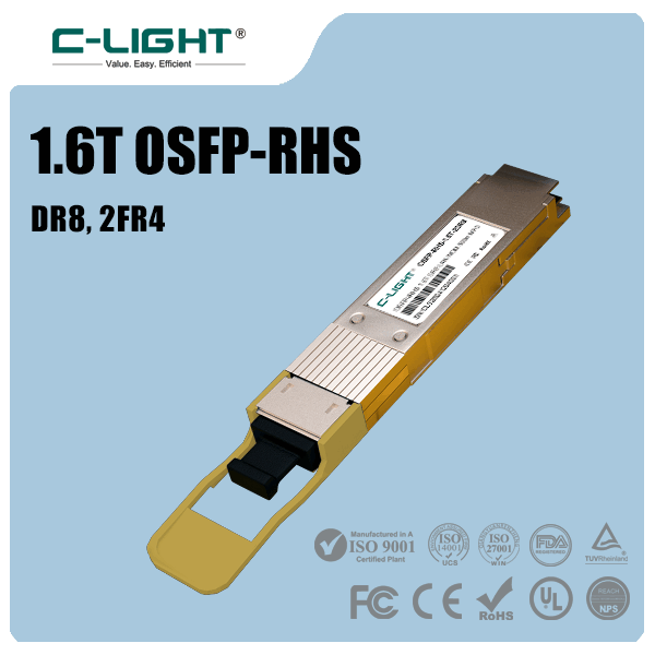
1.6T OSFP-RHS Optical Modules for platforms designed around the corresponding module interface.
800G Active Optical Cables for suitable short-reach optical interconnect applications.
800G Active Electrical Cables for compatible short-reach electrical connections.
These products represent pluggable optical and cable-based connectivity solutions, not photonic chiplets. Photonic chiplet integration represents a different level of system architecture and may complement conventional transceivers as AI infrastructure evolves.
11. What Will Determine the Commercial Adoption of Photonic Chiplets?
The long-term adoption of photonic chiplets will depend on more than optical bandwidth. AI system designers must evaluate the total cost, power consumption, reliability, packaging complexity, and software compatibility of the complete computing platform.
Several factors will influence commercial deployment:
System-level energy efficiency: The complete electrical-to-optical-to-electrical path must deliver meaningful efficiency improvements after accounting for laser power, drivers, receivers, cooling, and control circuits.
Manufacturing scalability: Photonic chiplets need repeatable production processes and sufficient packaging yield for large-volume deployment.
Standardized interfaces: Compatible die-to-die interfaces, optical connections, and management specifications can reduce integration barriers.
Reliability and serviceability: Systems need practical methods for monitoring, diagnosing, and replacing optical components.
Network architecture: Optical links must fit the communication protocols, switching topology, and memory architecture used by the AI platform.
Total system cost: The performance benefits must justify additional photonic components, fiber connections, packaging processes, and testing equipment.
Photonic chiplets are most likely to gain traction where electrical interconnect limitations create a clear system-level bottleneck. Their adoption will therefore vary by application, package size, communication distance, and required bandwidth.
12. Conclusion
Photonic chiplets are an important development in the evolution of AI computing infrastructure. By integrating optical communication functions into semiconductor packages, they can help connect processors, accelerators, switches, and distributed memory resources with higher bandwidth density and longer optical reach.
Their role is not to replace electronic processors or eliminate all electrical interconnects. Instead, photonic chiplets complement electrical chiplets by providing optical communication where high data rates and longer distances make electrical routing increasingly difficult.
Future progress will depend on silicon photonics, external and integrated laser technologies, advanced 2.5D and 3D packaging, efficient optical coupling, and standardized interfaces. As AI clusters continue to expand, photonic chiplets could become an important building block for optical I/O, NPO, CPO, and next-generation high-performance computing systems.
For high-speed optical connectivity solutions, visit the C-LIGHT Optical Transceiver portfolio or Contact C-LIGHT for product and technical information.
 >

 >
 >
 >
 >
 >
 >
 >