TEL:+86 132 6656 7067





AI accelerator performance increasingly depends on how efficiently processors exchange data. Modern GPUs and custom XPUs can execute enormous numbers of calculations, but distributed workloads require continuous communication between processors, memory systems, and other computing resources. As accelerator clusters grow, the electrical connections between these components face increasing challenges in bandwidth density, signal integrity, transmission distance, and power consumption.
Optical I/O addresses this challenge by moving electrical-to-optical conversion closer to the processor. Instead of carrying high-speed electrical signals across increasingly demanding circuit-board paths, an optical interface converts data into light and transmits it through fiber. This architecture creates opportunities for higher-bandwidth chip-to-chip communication, larger accelerator systems, and more flexible AI infrastructure.
1. What Is Optical I/O?
Optical I/O, or optical input/output, is an interface technology that uses optical signals to transfer data between computing components. It combines electronic processing with photonic transmission, allowing electrical data generated by a processor to be converted into light for communication over optical fiber.
A typical optical I/O architecture includes several functional components:
Electrical interface: Connects the processor or electronic chip to the optical I/O subsystem.
Electrical driver: Provides the electrical signals required to control optical transmitters.
Optical transmitter: Converts electrical data into optical signals through a modulator or laser-based transmission architecture.
Photonic integrated circuit (PIC): Provides optical functions such as modulation, waveguide routing, multiplexing, and signal distribution.
Optical receiver: Uses photodetectors to convert incoming optical signals back into electrical signals.
Fiber interface: Connects the optical I/O system to another processor, optical engine, or network component.
Optical I/O is not simply another name for an optical transceiver. A conventional pluggable transceiver is installed in a switch or network-device cage, while an optical I/O solution can be integrated much closer to the processor package. The objective is to reduce the electrical distance between computing silicon and optical conversion.
2. Why Future AI Accelerators Need Optical I/O
AI training and inference increasingly rely on distributed computing. A large model may be divided across multiple accelerators, with each processor handling a portion of the workload. These processors must exchange intermediate results, synchronize operations, and access shared or distributed memory.
As the number of accelerators increases, the communication requirements become more demanding. A processor with greater computational capacity does not automatically improve total system performance if its communication links cannot deliver data efficiently.
Traditional electrical interconnects remain effective for short connections. However, high-speed electrical signals experience insertion loss, crosstalk, reflections, and frequency-dependent distortion as channel length and signaling rates increase.
| AI Infrastructure Challenge | Electrical Interconnect Limitation | Potential Optical I/O Contribution |
|---|---|---|
| Increasing bandwidth | Higher signaling rates increase electrical channel complexity | Supports high-capacity transmission over optical channels |
| Longer communication distances | Signal degradation increases with electrical channel length | Fiber supports longer reach with lower transmission loss |
| Power consumption | Retimers, equalization, and signal conditioning add power | Can reduce some electrical-link overhead when conversion is placed closer to the processor |
| Interconnect density | Electrical routing and connector constraints limit practical scaling | Fiber routing enables high-capacity optical connections in compact spaces |
| System scalability | Extending electrical fabrics across larger systems becomes increasingly difficult | Can support larger processor and accelerator interconnection domains |
Optical I/O does not eliminate every electrical connection inside an AI accelerator. Processors still require electrical interfaces for local logic, memory, control, and photonic-device operation. Its value comes from replacing selected high-bandwidth electrical communication paths where optical transmission offers a better system-level trade-off.
3. How Optical I/O Works Inside an AI Accelerator
Optical I/O creates a communication path between electronic processing components and optical transmission channels. The architecture typically combines an electrical interface, optical engine, photonic components, and fiber connections.
A simplified transmit-and-receive process works as follows:
Data generation: The GPU, XPU, or other processor generates data for another computing component.
Electrical signaling: The processor sends the data through an electrical interface to the optical I/O circuitry.
Electro-optical conversion: Driver and modulator circuits encode the electrical information onto an optical carrier.
Optical transmission: The optical signal travels through a fiber connection toward the receiving component.
Optical detection: A photodetector converts the received optical signal into an electrical signal.
Data recovery: Receiver circuitry processes the electrical signal and delivers the recovered data to the destination processor.
In practical implementations, additional functions may be required, including clock recovery, signal conditioning, wavelength control, monitoring, and error management. The exact architecture depends on the optical interface, modulation format, lane rate, and packaging technology.
The location of the electro-optical conversion is especially important. Moving the optical engine closer to the processor reduces the length of the high-speed electrical path. This is one of the main reasons optical I/O is being considered for future accelerator packages.
4. Optical I/O Chiplets and Silicon Photonics
One important development direction is the optical I/O chiplet. Instead of integrating every photonic and electronic function into a single monolithic processor, manufacturers can use a separate optical subsystem that is packaged alongside the main computing silicon.
This approach allows electronic processing and photonic transmission functions to be developed using different manufacturing technologies. The optical chiplet can contain a photonic integrated circuit, while an accompanying electronic integrated circuit handles drivers, receivers, and control functions.
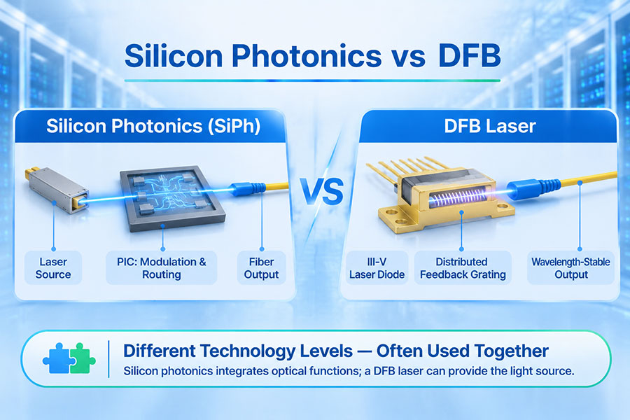
Silicon photonics is particularly relevant because it uses silicon-based waveguides and photonic structures to implement optical functions. It can support compact integration of modulators, optical couplers, multiplexers, and photodetectors. Laser sources may be integrated through heterogeneous processes or coupled from external sources, depending on the design.
Important advantages of optical I/O chiplet architectures include:
Closer integration between optical communication and processor silicon.
Shorter high-speed electrical paths between the processor and optical engine.
Potentially higher bandwidth density around the package.
Separation of photonic and electronic manufacturing processes.
More flexible optical connectivity for multi-chip accelerator systems.
However, chiplet-based optical I/O requires precise package integration, high-quality electrical connections, optical coupling, thermal management, and reliable assembly processes. The optical subsystem must operate within the mechanical and thermal limits of the processor package.
5. Optical I/O, Pluggable Optics, NPO, and CPO
Optical I/O is closely related to several optical integration architectures, but these terms describe different aspects of system design. Pluggable optics place the optical transceiver at the equipment front panel. NPO moves optical engines closer to the host ASIC, while CPO integrates optical engines within the same package or closely coupled package assembly as the electronic chip.
Optical I/O chiplets can be used as part of a CPO or other advanced packaging architecture. They are not restricted to one mechanical implementation.
| Architecture | Optical Integration Position | Main Characteristics | Typical Considerations |
|---|---|---|---|
| Pluggable Optics | Removable front-panel transceiver | Established optical connectivity with field-replaceable modules | Electrical channel length, module power, front-panel space |
| On-Board Optics (OBO) | Optical engine mounted on the system board | Shorter electrical paths than front-panel modules | Board integration and optical fiber management |
| Near-Packaged Optics (NPO) | Close to the ASIC or processor package | Reduces electrical connection distance while retaining some separation from the main package | Serviceability, optical routing, and thermal integration |
| Co-Packaged Optics (CPO) | Within or directly alongside the electronic chip package | Very short electrical paths between the ASIC and optical engines | Packaging, laser architecture, cooling, and repair strategy |
| Optical I/O Chiplet | Separate optical subsystem integrated into the computing package | Dedicated photonic and electronic functions for chip-level optical communication | Chiplet interfaces, package yield, optical coupling, and standards |
These approaches are complementary rather than mutually exclusive. For example, an optical I/O chiplet can form part of a co-packaged optical architecture, while pluggable transceivers continue to provide connections between switches and external network equipment.
6. How Optical I/O Can Improve AI Scale-Up Connectivity
Scale-up networking connects processors within a tightly integrated computing domain. It is designed to provide high-bandwidth communication between accelerators, often with strict requirements for latency, synchronization, and data-transfer efficiency.
Traditional scale-up systems commonly use electrical interconnects for short-distance communication. As the number of accelerators and the physical size of the computing system increase, extending these electrical connections becomes more challenging.
Optical I/O can provide an alternative for selected connections between accelerator packages, compute trays, or groups of processors. By moving optical conversion closer to the computing silicon, the system can use fiber to extend communication beyond the practical reach of some high-speed electrical channels.
This can support several architectural goals:
Connecting larger groups of accelerators without relying exclusively on long electrical channels.
Increasing the available communication bandwidth between compute domains.
Supporting more flexible rack-level and multi-rack scale-up architectures.
Reducing selected electrical signal-conditioning requirements.
Providing a foundation for disaggregated computing and memory architectures.
Optical I/O does not automatically make an accelerator cluster behave like a single processor. Software, communication protocols, memory consistency, switching architecture, and topology still determine how efficiently the system operates.
7. Optical I/O and the Evolution of Bandwidth Density
Bandwidth density measures how much data capacity can be delivered within a defined physical area or package boundary. As AI accelerator performance grows, the amount of data that must move between computing components also increases.
Traditional electrical interfaces face constraints from package pins, board routing, connector density, and channel losses. Optical I/O offers another way to distribute communication channels by using optical fibers and photonic interfaces.
The following table illustrates how different integration approaches change the location of the optical interface. It is a qualitative architectural comparison rather than a guaranteed performance ranking.
| Design Dimension | Traditional Electrical I/O | Pluggable Optical I/O | Integrated Optical I/O |
|---|---|---|---|
| Signal transmission | Electrical traces or cables | Electrical connection to a removable optical module, then fiber | Electrical connection to a nearby optical engine, then fiber |
| Optical conversion location | No optical conversion | Front-panel module | Near or within the processor package |
| Electrical channel length | Depends on board and cable routing | Can be relatively long between ASIC and module | Designed to be shorter |
| Fiber connectivity | Not required for the electrical link | External fiber connection | Fiber connected to package-level or board-level optical interfaces |
| Serviceability | Depends on connector and system design | Generally straightforward module replacement | More complex, depending on package and optical-engine architecture |
| Integration complexity | Established electrical packaging | Established module and host integration model | Requires advanced photonic packaging and thermal co-design |
The long-term objective is not simply to maximize the number of optical channels. It is to increase useful bandwidth while controlling energy per bit, latency, package complexity, and system cost.
8. Power Efficiency and Thermal Management
Energy efficiency is one of the strongest motivations for optical I/O. High-speed electrical links may require equalization, retiming, and signal conditioning to compensate for channel losses. These functions consume power and generate heat.
By shortening the electrical path and using optical transmission for longer connections, an integrated optical I/O architecture may reduce some of this overhead. However, the optical engine itself still requires electrical power for drivers, modulators, photodetectors, control circuits, and sometimes laser sources.
System-level efficiency therefore depends on several factors:
Electrical interface power: Energy consumed by the processor-side SerDes and optical-engine electronics.
Optical conversion efficiency: Power required to generate, modulate, and detect optical signals.
Laser architecture: Whether the design uses integrated, hybrid, or external laser sources.
Thermal coupling: Heat transfer between the optical engine, processor package, and cooling system.
Optical link performance: Coupling loss, fiber loss, receiver sensitivity, and required signal margin.
Thermal management is particularly challenging when optical engines are placed close to high-power AI processors. Photonic components may be sensitive to temperature changes, while the processor package can generate substantial heat. Thermal isolation, laser placement, package materials, and cooling architecture must be considered together.
9. Current Development Challenges for Optical I/O
Although optical I/O offers significant potential, several engineering challenges must be addressed before it can become a broadly deployed interface for AI accelerators.
Packaging complexity: Photonic and electronic components require precise alignment, interconnection, and assembly processes.
Thermal sensitivity: Optical components and laser sources must operate reliably near high-power processors.
Manufacturing yield: Integrating optical and electronic components introduces additional manufacturing and testing requirements.
Optical coupling: Efficient light transfer between photonic circuits, fiber arrays, and external optical components is essential.
Repair and replacement: Integrated optical engines may be more difficult to service than independent pluggable modules.
Interoperability: Electrical interfaces, optical specifications, management functions, and system-level protocols need consistent implementation.
Cost and supply chain: Photonic packaging, laser sources, specialized materials, and testing capacity must scale for high-volume deployment.
Standardization is also important. The Optical Internetworking Forum (OIF) has been developing work related to Compute Optics Interface (COI) and energy-efficient interfaces for AI scale-up. These activities address the electrical and optical interface requirements needed to build interoperable compute connectivity ecosystems.
10. Industry Development and Optical I/O Demonstrations
Optical I/O has moved beyond purely theoretical research, with semiconductor and photonics companies demonstrating integrated optical chiplets and developing architectures for future computing systems.
For example, Intel demonstrated an optical compute interconnect chiplet co-packaged with a CPU at OFC 2024. The demonstration supported up to 4 Tbps of bidirectional data transfer and used fiber connectivity to extend communication between computing platforms. It illustrated how silicon photonics could be integrated with electronic processing components for future AI and high-performance computing systems.
Industry development is also moving toward more formalized compute optical interfaces. In February 2026, OIF published a Compute Optics Interface white paper focused on optical scale-up connectivity. The work examines co-packaged and chiplet-based designs, onboard optics, pluggable architectures, and the trade-offs between electrical and optical interfaces.
These demonstrations and industry activities indicate growing interest in optical communication closer to the processor. However, a technology demonstration or interface framework should not be confused with universal commercial deployment. Product availability, interoperability, and system qualification remain dependent on individual implementations.
11. Optical I/O and C-LIGHT's High-Speed Optical Connectivity
Optical I/O operates close to the processor package, while pluggable optical transceivers and active cables provide connectivity across the wider data center network. These technologies serve different parts of the AI infrastructure and are complementary.
As accelerator systems adopt more integrated optical interfaces, high-speed external connectivity will remain essential for connecting servers, switches, racks, and data center network domains.
400G Optical Transceivers
400G optical modules support high-bandwidth switch-to-switch and server-to-network connections in established data center architectures.
800G Optical Transceivers
800G modules provide higher per-port bandwidth for next-generation switching systems and AI data center fabrics. Host compatibility, optical reach, and thermal requirements should be verified for each deployment.
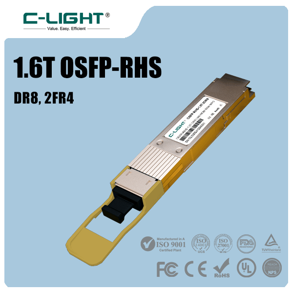
1.6T OSFP-RHS Optical Connectivity
1.6T OSFP-RHS addresses high-bandwidth optical connectivity in compatible host platforms using a riding heat-sink thermal architecture.
800G Active Optical and Electrical Cables
Active cable solutions support short-reach connections between network devices and computing equipment. AOC uses optical transmission, while AEC uses active electrical signal conditioning.
These products should be viewed as external network connectivity options rather than optical I/O chiplets integrated directly into AI accelerator packages. The distinction matters when designing a complete AI network that combines processor-level optical links with switch-level and rack-level optical connections.
12. What Is the Future Role of Optical I/O in AI Accelerators?
Optical I/O is expected to become increasingly important as AI processors move toward higher bandwidth, larger multi-chip packages, and more distributed computing architectures. Its role will extend beyond conventional switch-to-switch communication toward processor-level and package-level connectivity.
Several development directions are likely to shape its adoption:
Higher optical bandwidth per package: Future accelerator platforms will require more optical channels and higher aggregate bandwidth to support communication among computing components.
More integrated photonics: Optical chiplets and silicon photonic engines will move closer to processor and memory interfaces.
Expanded scale-up fabrics: Optical links may allow computing systems to connect larger groups of accelerators across multiple packages and racks.
Improved energy efficiency: Reducing electrical channel length and optimizing electro-optical conversion will be important for controlling interconnect power.
More standardized interfaces: Common electrical, optical, and management specifications will help improve interoperability across the ecosystem.
Hybrid network architectures: Copper, pluggable optics, optical I/O chiplets, and co-packaged optics will coexist according to distance, performance, and serviceability requirements.
Optical I/O is not expected to replace all electrical communication inside processors. Short-distance electrical links will continue to serve many package-level functions, while optical interfaces will become more attractive where bandwidth density, reach, and energy requirements justify the additional photonic integration.
13. Conclusion
Optical I/O is becoming an important building block for future AI accelerator architectures. By moving optical conversion closer to computing silicon, it can reduce the distance traveled by high-speed electrical signals and create new opportunities for bandwidth scaling, energy efficiency, and larger accelerator interconnection domains.
Silicon photonics, optical I/O chiplets, NPO, and CPO are contributing to this transition, although each introduces different integration, thermal, manufacturing, and serviceability requirements. Their adoption will depend on system-level performance and the maturity of interoperable interfaces.
For AI infrastructure, the future will not depend on one optical technology alone. Processor-level optical I/O, high-speed pluggable transceivers, active cables, and optical transport systems will work together to connect computing resources from individual packages to large data center networks. C-LIGHT supports high-speed optical connectivity across 400G, 800G, and 1.6T product generations. For product specifications and application support, Contact C-LIGHT.
 >

 >
 >
 >
 >
 >
 >
 >