TEL:+86 132 6656 7067





The semiconductor industry is moving beyond conventional monolithic chip designs toward architectures that combine multiple specialized dies within a single package. As artificial intelligence, high-performance computing, and data center networks demand greater communication bandwidth, optical chiplet technology is emerging as a way to integrate photonic functions directly into advanced semiconductor packages.
Optical chiplets combine optical communication components with electronic processing and control circuits. They can provide high-speed optical interfaces for processors, switches, and accelerator systems while reducing dependence on long, high-speed electrical connections. By combining silicon photonics, heterogeneous integration, and advanced packaging, this technology creates a path toward more scalable optical I/O and co-packaged optics architectures.
1. What Is Optical Chiplet Technology?
Optical chiplet technology is an integration approach in which photonic components are fabricated as separate semiconductor dies and assembled with electronic chips or other components within a common package.
An optical chiplet typically contains some or all of the photonic functions required for optical communication. These may include optical modulation, photodetection, wavelength multiplexing, optical routing, and fiber coupling. Depending on the architecture, the chiplet can also be integrated with electronic driver and receiver circuits or connected to separate electronic dies.
A typical optical chiplet system may include:
Photonic Integrated Circuit (PIC): Contains optical waveguides, modulators, photodetectors, couplers, and other light-processing components.
Electronic Integrated Circuit (EIC): Provides electrical drivers, transimpedance amplifiers, signal conditioning, and control functions.
Laser source: Supplies the optical carrier through an integrated, hybrid, heterogeneous, or external laser arrangement.
Interposer or package substrate: Connects the optical and electronic dies through electrical routing and mechanical support.
Optical interface: Connects the photonic chiplet to fiber arrays, optical waveguides, or other photonic components.
Thermal management structure: Controls heat generated by electronic and optical components.
The main idea is to separate complex semiconductor functions into specialized dies and combine them through advanced packaging. Electronic chips continue to handle computation and signal processing, while optical chiplets provide the communication interface.
2. Why Is Optical Chiplet Technology Needed?
Traditional semiconductor scaling has relied heavily on increasing transistor density and improving the performance of individual processors. However, modern computing systems increasingly face a different limitation: moving data between chips can be as challenging as processing the data itself.
AI accelerators, high-performance CPUs, memory systems, and network switches exchange large volumes of information. As aggregate bandwidth increases, electrical interconnects encounter several engineering constraints.
Electrical signal loss: High-frequency signals experience increasing insertion loss as they travel through package traces and circuit-board connections.
Signal integrity: Crosstalk, impedance discontinuities, and frequency-dependent distortion make high-speed electrical routing more difficult.
Power consumption: High-speed electrical interfaces may require substantial driver, equalization, and retiming power.
Routing density: Increasing the number of electrical channels requires more package connections and routing resources.
Scalability: Larger AI systems need communication links that can extend beyond the physical limits of a single semiconductor package.
Optical chiplets address these challenges by moving electrical-to-optical conversion closer to the computing or switching chip. Data can then travel through optical fibers or waveguides, supporting high-bandwidth communication over distances that are difficult to serve efficiently with conventional electrical routing.
3. How Does Optical Chiplet Technology Work?
An optical chiplet acts as an interface between an electronic computing device and an optical communication network. It converts electrical data into optical signals for transmission and converts incoming optical signals back into electrical data at the receiving end.
A simplified optical transmission process includes the following stages:
Data generation: A processor, GPU, accelerator, or switch ASIC generates digital data.
Electrical transfer: The data travels through a short electrical connection from the host chip to the optical chiplet.
Signal conditioning: Electronic driver circuits prepare the electrical signal for optical modulation.
Optical modulation: A photonic modulator encodes the electrical data onto light supplied by a laser source.
Optical transmission: The modulated light travels through an optical waveguide or fiber connection.
Optical detection: A photodetector at the receiving endpoint converts the incoming light into an electrical signal.
Data recovery: Receiver electronics process the recovered signal and deliver the data to the destination chip.
For bidirectional communication, each endpoint generally requires suitable transmitting and receiving functions. The physical architecture may use separate transmit and receive fibers, wavelength-division multiplexing, or other optical channel arrangements.
The optical chiplet does not independently perform the processor's computation. Its primary function is to provide the optical communication path that connects electronic systems.
4. Main Components of an Optical Chiplet
The design of an optical chiplet depends on its intended application, data rate, optical interface, and integration method. Several core components determine its performance.
| Component | Function | Engineering Importance |
|---|---|---|
| Optical modulator | Encodes electrical data onto an optical carrier | Influences bandwidth, drive voltage, optical loss, and signal quality |
| Photodetector | Converts received optical signals into electrical signals | Affects receiver sensitivity, bandwidth, and noise performance |
| Optical waveguide | Guides light within the photonic circuit | Determines optical routing and propagation loss |
| Laser source | Generates the optical carrier | Determines available optical power, wavelength, and source stability |
| WDM multiplexer | Combines multiple optical wavelengths | Increases aggregate bandwidth through shared optical paths |
| WDM demultiplexer | Separates incoming wavelengths | Routes optical channels to their corresponding receivers |
| Optical coupler | Transfers light between the chip and an external optical interface | Influences coupling efficiency and insertion loss |
| Electronic driver and receiver | Controls modulation and processes detected signals | Determines electrical interface performance and power consumption |
Not every optical chiplet contains all these components. For example, a design using an external continuous-wave laser may not include its own integrated laser. Some architectures also place the driver and receiver electronics on separate EIC dies rather than integrating them directly with the PIC.
5. Silicon Photonics and Heterogeneous Integration
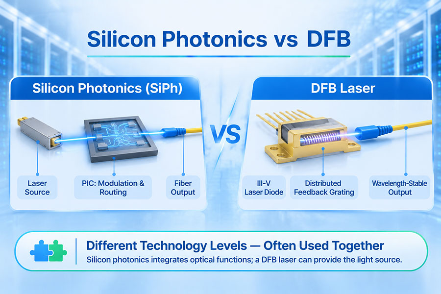
Silicon photonics is one of the most important technologies supporting optical chiplet development. It uses semiconductor fabrication techniques to create optical waveguides, modulators, couplers, and photodetectors on silicon-based platforms.
Silicon is attractive because its manufacturing ecosystem is closely related to established CMOS semiconductor processes. It supports dense photonic integration and can be combined with electronic chips through advanced packaging.
However, silicon does not efficiently generate light by itself because it is an indirect-bandgap material. Laser sources therefore often require other semiconductor materials or separate laser modules.
Heterogeneous integration addresses this limitation by combining different material systems within a common photonic platform. Examples include:
Silicon: Provides waveguides, passive optical routing, and integration with semiconductor manufacturing processes.
Indium phosphide (InP): Supports laser generation, optical amplification, and other active photonic functions.
Germanium: Can be used for photodetectors integrated with silicon photonic platforms.
Silicon nitride (SiN): Provides low-loss waveguides for applications requiring efficient optical routing.
Thin-film lithium niobate (TFLN): Offers strong electro-optic properties for high-speed modulation applications.
Different materials can be integrated through bonding, die attachment, transfer techniques, or other heterogeneous manufacturing processes. The appropriate approach depends on the optical functions, process compatibility, and production requirements.
Heterogeneous integration is not the same as simply placing multiple finished chips inside one package. It describes the integration of different material systems or semiconductor technologies, while packaging describes how the resulting components are assembled and connected.
6. Optical Chiplets vs. Traditional Optical Transceivers
Optical chiplets and conventional optical transceivers both provide optical communication functions, but they are designed for different integration levels.
| Feature | Optical Chiplet | Traditional Optical Transceiver |
|---|---|---|
| Integration level | Designed for integration within an advanced semiconductor package or optical engine | Designed as a complete module installed in a host equipment port |
| Host connection | Package-level electrical and optical interfaces | Standardized host electrical interface and external fiber interface |
| Primary application | Optical I/O, CPO, NPO, and advanced computing interconnects | Switch-to-switch, server-to-switch, and other network links |
| Serviceability | Depends on package design and chiplet replacement strategy | Generally replaceable as a pluggable module |
| Manufacturing focus | Die integration, optical coupling, advanced packaging, and chiplet testing | Module assembly, optical alignment, host compatibility, and module qualification |
| System architecture | Can place optical conversion close to the processor or ASIC | Usually places optical conversion at a removable equipment interface |
A conventional 800G or 1.6T optical transceiver is a complete optical module with its own mechanical form factor and host interface. An optical chiplet is a component intended to be integrated into a larger package.
Although both may use silicon photonics, modulators, photodetectors, and optical fibers, they should not be treated as interchangeable product categories.
7. Optical Chiplets and CPO, NPO, and Optical I/O
Optical chiplet technology is closely related to emerging optical interconnect architectures. However, these terms describe different aspects of system design.
| Technology | Definition | Relationship to Optical Chiplets |
|---|---|---|
| Optical chiplet | A specialized photonic die designed for integration with other semiconductor components | The physical photonic component |
| Optical I/O | An optical input/output interface for transferring data between computing components | Can be implemented using optical chiplets |
| CPO | Co-packaged optics, placing optical engines within or very close to an ASIC package | Optical chiplets can form part of the co-packaged optical engine |
| NPO | Near-packaged optics, positioning optical engines near the main ASIC package | Optical chiplets can be used within the nearby optical engine |
| Pluggable optics | Removable optical modules installed in equipment ports | A different integration architecture, although similar photonic technologies may be used internally |
In CPO, photonic components are positioned close to the switch ASIC to reduce the electrical distance between the switching chip and optical engine. In optical I/O applications, optical chiplets can provide communication interfaces for CPUs, GPUs, AI accelerators, or custom processors.
The distinction matters because an optical chiplet does not automatically imply CPO. It can also be used in other advanced packaging arrangements, including near-package optical engines and processor-focused optical I/O systems.
8. Advanced Packaging Technologies for Optical Chiplets
Packaging determines how photonic and electronic dies are physically and electrically connected. Unlike conventional electronic chiplets, optical chiplets also require carefully designed optical interfaces and stable fiber connections.
Several packaging technologies are relevant:
2.5D integration: Multiple dies are mounted on a common interposer or advanced substrate. This arrangement supports dense connections between the processor, EIC, and PIC.
3D integration: Dies are stacked vertically to increase integration density and shorten selected interconnect paths. Thermal management and manufacturing complexity become more demanding as components are placed closer together.
Flip-chip bonding: Semiconductor dies are mounted with their electrical contacts facing the substrate, supporting compact connections and short electrical paths.
Hybrid bonding: Fine-pitch bonding can create dense electrical and mechanical connections between semiconductor components.
Fiber array attachment: Multiple optical fibers are aligned with the photonic chip's input and output interfaces. Accurate positioning is essential for controlling optical coupling loss.
Optical interposer integration: Optical routing structures can be incorporated into suitable interposer or package designs to support optical connections between components.
These methods can be combined within a single package. The design must balance electrical performance, optical coupling, thermal behavior, mechanical stability, and manufacturing yield.
9. Applications of Optical Chiplet Technology
Optical chiplets have potential applications across several areas of computing and communication infrastructure.
AI accelerators: Optical I/O chiplets can connect GPUs and other AI processors to high-bandwidth communication fabrics, helping address the growing data movement requirements of distributed AI workloads.
High-performance computing: HPC systems can use optical chiplets to connect processors, memory resources, and networking components across larger system configurations.
Data center switches: Optical chiplets can be integrated into CPO architectures, shortening electrical paths between switch ASICs and optical interfaces.
Scale-up networks: Optical connections can support high-bandwidth communication between processors and accelerators within a tightly connected computing system.
Scale-out networks: Optical interfaces can support connections between servers, racks, and larger data center network segments.
Disaggregated computing: Optical interconnects may support more flexible placement of processing and memory resources, although system protocols, memory controllers, and latency requirements remain important constraints.
These applications have different requirements. A photonic chiplet designed for short-reach processor-to-processor communication may use a different optical architecture from one designed for a switch ASIC or a longer-reach network interface.
10. Key Technical Challenges
Optical chiplets offer a path toward denser optical integration, but their development requires progress across photonics, semiconductor packaging, thermal engineering, and manufacturing.
Optical coupling loss: Light must transfer efficiently between the photonic chiplet and external fibers or optical waveguides. Poor alignment can reduce available optical power and limit system reach.
Laser integration: Silicon photonics requires a suitable light source. Integrated, heterogeneous, hybrid, and external laser approaches each have different manufacturing and thermal implications.
Thermal management: Electronic processors generate heat that can affect nearby photonic components. Temperature control is important for laser wavelength stability, modulator performance, and long-term reliability.
Electrical signal integrity: The connection between the processor and photonic chiplet must support the required data rate with controlled insertion loss, crosstalk, and impedance behavior.
Manufacturing yield: Optical and electronic dies require different fabrication and testing processes. A defect in bonding, fiber attachment, or an electrical connection can affect the complete package.
Testing and repair: Optical chiplets need optical testing in addition to conventional electrical testing. Repairing an integrated photonic component may be more difficult than replacing a conventional pluggable module.
Interoperability: Different chiplets must work with compatible electrical interfaces, optical wavelengths, fiber connections, package dimensions, and management functions.
Cost and production scale: Advanced substrates, precision optical alignment, bonding equipment, and specialized testing can increase manufacturing costs. High-volume adoption will depend on repeatable processes and acceptable production yield.
11. Industry Development and Future Technology Directions
Research and industry development are increasingly focused on integrating photonic and electronic components into scalable packages. Several technology directions are shaping the optical chiplet ecosystem.
Higher optical bandwidth density: Future optical engines aim to increase the amount of data transmitted through a given package edge or fiber interface. Wavelength-division multiplexing and higher-speed optical lanes are important approaches.
Advanced heterogeneous integration: Combining silicon photonics with III-V materials, silicon nitride, and specialized electro-optic materials can expand the range of functions available within optical chiplets.
External laser architectures: Separating laser generation from the photonic package can improve thermal isolation and allow independent source maintenance in suitable systems.
Hybrid bonding and 3D packaging: Fine-pitch connections and vertical integration can support denser photonic-electronic assemblies.
Optical I/O for computing: Processor-focused optical chiplets may extend optical communication closer to CPUs, GPUs, and AI accelerators rather than limiting optical conversion to network switches.
Manufacturable optical interfaces: Improvements in fiber attachment, passive alignment, optical coupling, and wafer-level testing will be important for large-scale production.
Research roadmaps also illustrate the scale of future ambitions. For example, imec's optical interconnect program has identified development targets extending from 1.6T and 3.2T optical engines toward 6.4T and 12.8T, alongside higher bandwidth density and lower energy-per-bit goals. These are technology research targets, not specifications that should be assumed for currently available commercial products.
As optical chiplet technology matures, its role may expand from switch-focused CPO to broader processor-to-processor and accelerator-to-accelerator communication. The speed of adoption will depend on package economics, reliability, standardization, and demonstrated system-level advantages.
12. Optical Chiplets and C-LIGHT High-Speed Optical Connectivity
Optical chiplets represent an emerging semiconductor integration approach, while conventional optical transceivers remain essential for connecting data center switches, servers, and network equipment.
C-LIGHT's high-speed optical connectivity portfolio includes products for current data center and network infrastructure:
400G QSFP-DD Optical Transceivers for compatible 400G host platforms.
400G OSFP Optical Transceivers for supported OSFP-based equipment.
800G QSFP-DD Optical Transceivers for high-bandwidth data center links.
800G OSFP Optical Transceivers for compatible 800G network systems.
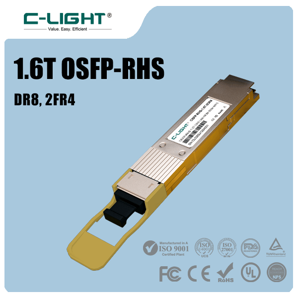
1.6T OSFP-RHS Optical Modules for systems designed around the corresponding module interface.
800G Active Optical Cables for suitable short-reach optical connections.
800G Active Electrical Cables for compatible short-reach electrical interconnects.
These products serve conventional optical module and cable-based connectivity applications. They should not be described as optical chiplets or CPO components unless a specific product is independently confirmed to use that architecture.
As data center networks evolve, conventional pluggable optics and emerging optical chiplet architectures are likely to serve complementary roles. Pluggable modules provide replaceable network interfaces, while optical chiplets target deeper integration between photonic and electronic components.
13. Conclusion
Optical chiplet technology combines photonic functions with advanced semiconductor packaging to provide high-bandwidth optical interfaces for computing and communication systems. By integrating PICs with electronic components, it can bring optical conversion closer to processors, switches, and AI accelerators.
Its development depends on silicon photonics, heterogeneous material integration, laser-source design, advanced packaging, precise optical coupling, and reliable manufacturing. These technologies create a foundation for optical I/O, CPO, NPO, and future high-performance computing architectures.
Optical chiplets will not eliminate the need for conventional optical transceivers or electrical interconnects. Instead, they will extend the available design options, allowing system architects to choose electrical or optical communication according to bandwidth, distance, power, and integration requirements.
For high-speed optical connectivity solutions, visit the C-LIGHT Optical Transceiver portfolio or Contact C-LIGHT for product and technical information.
 >

 >
 >
 >
 >
 >
 >
 >