TEL:+86 132 6656 7067





Modern optical communication systems require more than high-performance waveguides. They also need efficient light sources, optical amplifiers, high-speed modulators, photodetectors, and reliable electrical interfaces. Although silicon photonics provides a scalable platform for integrating many optical functions, silicon alone cannot efficiently perform every photonic function required by a complete optical communication system.
Heterogeneous integration addresses this limitation by combining silicon photonic circuits with devices or material layers made from other semiconductor and optical materials. This approach brings complementary capabilities together, allowing a single photonic platform to support more complex optical functions. It is becoming increasingly important in the development of compact optical engines, high-speed transceivers, coherent communication systems, and next-generation data center interconnects.
1. What Is Heterogeneous Integration in Silicon Photonics?
Heterogeneous integration in silicon photonics is a manufacturing and integration approach that combines different material systems within a common photonic platform. Instead of relying entirely on silicon, engineers introduce materials with optical or electrical properties that silicon does not provide as efficiently.
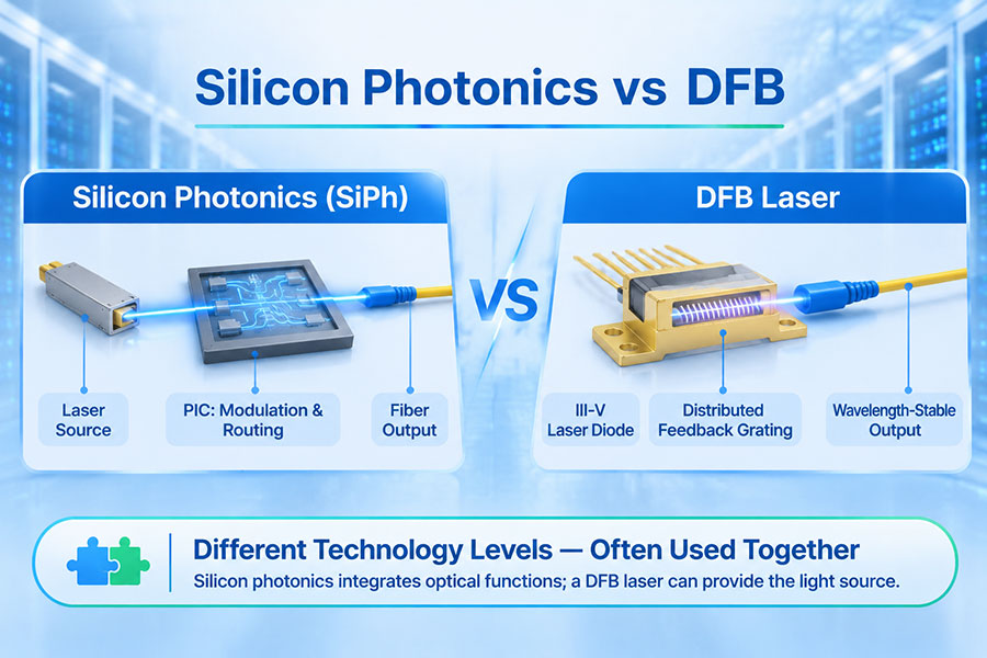
A typical example is integrating III-V semiconductor materials, such as indium phosphide (InP) or gallium arsenide (GaAs), with a silicon photonic integrated circuit. Silicon provides waveguides and passive optical routing, while III-V materials can provide light generation and optical gain.
Depending on the architecture, heterogeneous integration can also incorporate other materials, including:
Indium phosphide (InP): Used for semiconductor lasers, optical amplifiers, and other active photonic devices.
Gallium arsenide (GaAs): Used in selected light-emitting and photonic device structures.
Thin-film lithium niobate (TFLN): Provides strong electro-optic properties for high-speed modulation.
Barium titanate (BTO): Investigated for electro-optic modulation and other integrated photonic functions.
Silicon nitride (SiN): Provides low-loss waveguides and is frequently used in multi-material photonic integration.
The objective is not simply to place multiple chips next to one another. It is to integrate complementary materials and devices so that optical signals can move efficiently between different functional regions of a photonic circuit.
2. Why Does Silicon Photonics Need Heterogeneous Integration?
Silicon photonics benefits from mature semiconductor manufacturing processes and the ability to create dense optical waveguide circuits. Silicon-on-insulator (SOI) platforms can support waveguides, splitters, couplers, resonators, filters, and certain types of optical modulators.
However, silicon has an indirect bandgap, making efficient light emission difficult. This creates a challenge when designers want to integrate a complete optical transmitter and receiver on a common silicon photonic platform.
Other limitations also influence material selection:
Silicon does not provide the same efficient laser functionality as direct-bandgap III-V semiconductor materials.
Different materials offer different electro-optic coefficients and modulation mechanisms.
Some applications require lower optical propagation loss or specialized nonlinear optical properties.
High-performance photonic systems may need different materials for light generation, modulation, amplification, and detection.
Heterogeneous integration allows engineers to select the most appropriate material for each function rather than forcing every component to use one semiconductor platform.
3. How Does Heterogeneous Integration Work?
Heterogeneous integration can be implemented through several manufacturing approaches. The selected method depends on the material combination, device architecture, required alignment accuracy, thermal budget, manufacturing scale, and production cost.
A common III-V-on-silicon integration process involves the following stages:
Silicon photonic circuit fabrication: Silicon waveguides, optical couplers, and passive components are fabricated on a silicon-on-insulator wafer.
Preparation of the active material: A III-V semiconductor layer or device structure is prepared for integration.
Bonding or material transfer: The III-V material is attached to the silicon photonic platform using a suitable bonding or transfer process.
Device definition: Additional lithography and fabrication steps create lasers, amplifiers, or other active photonic components.
Electrical and optical connection: Electrodes, contacts, waveguides, and coupling structures are completed.
Testing and qualification: The integrated photonic device is evaluated for optical performance, electrical behavior, thermal stability, and reliability.
In wafer-scale approaches, multiple devices can be processed across a wafer rather than assembled individually. This can improve alignment consistency and manufacturing throughput, although actual yield depends on bonding quality, material compatibility, and process control.
4. Main Heterogeneous Integration Technologies
Several technologies are used to combine different material systems with silicon photonics. They offer different levels of integration density, process complexity, and manufacturing scalability.
| Integration method | Basic principle | Advantages | Main challenges |
|---|---|---|---|
| Wafer-to-wafer bonding | Joins two wafers to form a combined material platform | Potential for large-area and high-density integration | Wafer compatibility, surface quality, bonding defects, and yield |
| Die-to-wafer bonding | Attaches individual dies to a target wafer | Flexible material and device selection | Placement accuracy, throughput, and assembly complexity |
| Direct bonding | Joins prepared surfaces without a conventional adhesive layer | Can provide close material contact and compact interfaces | Strict surface cleanliness, flatness, and process requirements |
| Adhesive bonding | Uses an intermediate bonding material between dissimilar surfaces | Can accommodate certain surface and material differences | Thermal properties, adhesive thickness, and long-term stability |
| Micro-transfer printing | Transfers small prefabricated devices onto a target photonic substrate | Selective placement and efficient use of functional materials | Transfer accuracy, device handling, and production throughput |
| Selective epitaxial integration | Grows a material structure on selected regions of a silicon-based platform | Potential for closely integrated active devices | Lattice mismatch, defects, and process compatibility |
These methods are not interchangeable. Wafer bonding and micro-transfer printing are particularly relevant to integrating dissimilar material layers or devices. Selective epitaxial growth can also create integrated structures, but it involves different materials engineering and fabrication challenges.
5. The Role of III-V Materials in Silicon Photonics
III-V semiconductor materials are among the most important additions to silicon photonic platforms because they enable efficient optical gain and light generation.
InP-based devices are especially relevant to optical communication because they can support semiconductor lasers and optical amplifiers at telecommunications wavelengths. When integrated with silicon waveguides, these active devices can provide optical functionality that is difficult to achieve using silicon alone.
Typical III-V functions include:
Integrated lasers: Generate the optical carrier used for data transmission.
Semiconductor optical amplifiers (SOAs): Amplify optical signals within a photonic circuit.
Electro-absorption modulators: Control optical intensity through electrically induced changes in absorption.
Active photonic devices: Support specialized optical functions in integrated transmitter and receiver architectures.
One important benefit is that the silicon waveguide can route light between different functional devices. This makes it possible to combine an active III-V region with passive silicon photonic circuitry in a compact architecture.
6. Heterogeneous Integration vs. Hybrid Integration vs. Monolithic Integration
Heterogeneous, hybrid, and monolithic integration are related concepts, but they describe different manufacturing strategies. The terminology is not completely consistent across all research papers and industry publications, so the actual fabrication process should always be considered.
| Integration approach | Manufacturing concept | Typical example | Main characteristic |
|---|---|---|---|
| Monolithic integration | Multiple functions are fabricated within a common material and process platform | Silicon waveguides and integrated silicon-based devices | High process integration, subject to material and process limitations |
| Heterogeneous integration | Dissimilar materials or material layers are bonded or transferred onto a common photonic platform | III-V gain material integrated with silicon waveguides | Combines complementary material properties within an integrated circuit |
| Hybrid integration | Separately fabricated optical components or chips are assembled and optically connected | An InP laser die coupled to a silicon photonic chip | Allows separate component fabrication and testing before assembly |
For example, an InP laser die mounted and optically coupled to a silicon photonic chip during packaging is commonly described as hybrid integration. Bonding a III-V material layer onto a silicon wafer and then fabricating the active laser structure through subsequent processing is commonly described as heterogeneous integration.
Some publications use these terms more broadly or interchangeably. For technical evaluation, the bonding sequence, material transfer method, and stage of device fabrication provide a more reliable description than the terminology alone.
7. Applications in Optical Transceivers and Data Center Networks
Optical transceivers combine electrical interfaces, optical transmitters, optical receivers, and signal-processing functions. As data rates increase from 400G to 800G and 1.6T, designers need optical components with higher bandwidth, improved integration density, and predictable performance.
Heterogeneous silicon photonics can contribute to this development by combining optical functions that would otherwise require separate components.
Potential applications include:
High-speed optical transmitters: Integrated laser sources and modulators can support compact transmitter architectures.
Optical receivers: Integrated waveguides and photodetector structures can support signal routing and detection.
Wavelength multiplexing: Integrated filters and multiplexers can combine multiple optical channels.
Coherent optical engines: Multiple photonic functions can be integrated to support complex modulation and coherent transmission.
AI data center connectivity: More integrated optical engines can help address bandwidth density, power, and packaging requirements in large-scale networks.
Heterogeneous integration does not determine the Ethernet data rate or host compatibility of a transceiver by itself. Those characteristics depend on the complete module design, electrical interface, optical specification, firmware or module coding, and host platform.
8. Heterogeneous Integration in 800G and 1.6T Optical Engines
The development of 800G and 1.6T optical connectivity increases the importance of photonic integration. Higher data rates require more capable electrical and optical components, while compact module designs place greater pressure on thermal and power budgets.
Heterogeneous integration can support these requirements by bringing lasers, amplifiers, modulators, and passive optical routing closer together. Depending on the implementation, it may reduce the number of discrete optical components and simplify certain optical connections.
However, integration does not automatically eliminate the need for high-performance DSPs, driver circuits, receiver electronics, or thermal management. These functions remain part of the overall transceiver architecture.
C-LIGHT's current optical connectivity portfolio includes:
800G OSFP Optical Transceivers for supported high-bandwidth network platforms.
800G QSFP-DD Optical Transceivers for compatible 800G switch and router interfaces.
400G QSFP-DD Optical Transceivers for 400G network infrastructure.
400G OSFP Optical Transceivers for supported OSFP-based systems.
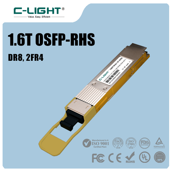
1.6T OSFP-RHS for next-generation high-bandwidth platforms that support the corresponding interface and thermal design.
These products represent optical connectivity solutions at their respective data rates. Their inclusion here does not imply that every model uses heterogeneous silicon photonic integration. The internal photonic architecture and material platform must be confirmed through the specifications of each individual product.
9. Benefits of Heterogeneous Integration
The main advantage of heterogeneous integration is the ability to combine material systems according to their functional strengths. This can improve the overall capability of a photonic integrated circuit.
More complete optical functionality: Silicon waveguides can be combined with III-V lasers and amplifiers, allowing more optical functions to be integrated on a common platform.
Greater integration density: Bonding and transfer technologies can reduce the need for separately packaged components and their associated optical interfaces.
Design flexibility: Engineers can select different materials for light generation, modulation, amplification, and passive routing.
Potential manufacturing scalability: Wafer-level bonding and processing can support repeatable fabrication across multiple devices, provided that yield and process control are sufficiently mature.
Support for advanced optical architectures: Multi-material integration can contribute to compact coherent engines, wavelength-multiplexed devices, and future optical interconnects.
10. Technical Challenges and Manufacturing Limitations
Despite its advantages, heterogeneous integration introduces manufacturing challenges that must be solved before a photonic platform can achieve consistent high-volume production.
Material compatibility: Different semiconductor materials have different lattice constants, thermal expansion coefficients, chemical properties, and processing requirements. These differences complicate direct integration.
Bonding quality: Surface contamination, roughness, voids, and bonding defects can affect device performance and long-term reliability. High-quality bonding requires careful surface preparation and process control.
Optical coupling efficiency: Light must transfer efficiently between dissimilar waveguides and active regions. Poor mode matching or alignment can increase insertion loss and reduce system efficiency.
Thermal management: Lasers and amplifiers generate heat. Temperature changes can affect wavelength stability, output power, and device lifetime. Thermal design becomes more complicated when active and passive materials are closely integrated.
Manufacturing yield: Integrating several material systems creates more process steps and potential failure points. A defect in one region can affect the performance of the complete photonic circuit.
Testing and reliability: Integrated devices require appropriate wafer-level testing, optical characterization, environmental qualification, and long-term reliability evaluation.
11. Heterogeneous Integration and the Future of Silicon Photonics
As optical communication moves toward 1.6T and future 3.2T-class architectures, the need for more capable photonic integration platforms will continue to grow. Heterogeneous integration is one of the approaches that can help address the limitations of single-material photonic circuits.
Several development directions are particularly important:
III-V-on-silicon lasers: Improved integration processes can support more compact optical sources and laser arrays.
Advanced electro-optic materials: TFLN and other materials can add modulation capabilities that complement silicon-based devices.
Multi-material photonic circuits: Silicon, silicon nitride, III-V semiconductors, and other materials can be combined to provide different optical functions.
Wafer-scale manufacturing: Higher-throughput bonding and transfer processes may improve production economics and integration consistency.
Advanced packaging: Photonic chips, electronic driver circuits, and optical interfaces will need more sophisticated packaging and thermal solutions.
AI optical interconnects: Integrated photonic engines may become increasingly important in high-bandwidth accelerator and switch architectures.
Heterogeneous integration may also support the development of near-packaged optics (NPO) and co-packaged optics (CPO). These architectures focus on placing optical engines closer to switching or computing ASICs. Heterogeneous integration can provide the material and device building blocks, while NPO and CPO describe broader system-level placement and packaging approaches. They are related, but they are not the same concept.
12. Conclusion
Heterogeneous integration is an important technology for expanding the capabilities of silicon photonics. By combining silicon waveguides with III-V semiconductor lasers, optical amplifiers, advanced modulators, and other functional materials, engineers can build photonic circuits that offer more complete optical functionality than single-material platforms.
Wafer bonding, die-to-wafer bonding, direct bonding, adhesive bonding, and micro-transfer printing provide different ways to combine these materials. Each method involves trade-offs in alignment, optical loss, process compatibility, manufacturing yield, and cost.
As 400G, 800G, and 1.6T optical connectivity develops toward higher bandwidth and denser integration, heterogeneous photonic platforms will play an increasingly important role in optical engine design. Their commercial success will depend on reliable fabrication, efficient optical coupling, thermal control, and scalable manufacturing.
For current optical connectivity requirements, visit the C-LIGHT Optical Transceiver portfolio or Contact C-LIGHT for product and technical information.
 >

 >
 >
 >
 >
 >
 >
 >