TEL:+86 132 6656 7067





As optical communication systems move toward 800G, 1.6T, and higher bandwidth generations, packaging is becoming a critical part of overall system performance. Optical engines must combine photonic integrated circuits, electronic driver components, laser sources, fiber interfaces, and thermal structures within increasingly compact spaces. Even when individual optical and electronic chips deliver excellent performance, poor integration can introduce signal loss, alignment errors, thermal instability, and manufacturing yield problems.
Advanced optical packaging addresses these challenges by integrating photonic and electronic components into reliable, high-density assemblies. It provides the physical and electrical connections that allow optical devices to operate as a complete system. Its importance is growing across silicon photonics, high-speed optical transceivers, coherent optical engines, near-packaged optics (NPO), and co-packaged optics (CPO).
1. What Is Advanced Optical Packaging?
Advanced optical packaging refers to the technologies and manufacturing processes used to assemble, connect, protect, and manage optical and electronic components within a photonic device or system.
Unlike conventional electronic packaging, optical packaging must manage both electrical and optical interfaces. Electrical connections carry high-speed signals between integrated circuits, while optical interfaces guide light between photonic chips, waveguides, lasers, and external fibers.
A typical advanced optical package may contain:
Photonic Integrated Circuit (PIC): Performs optical functions such as modulation, wavelength multiplexing, optical routing, and photodetection.
Electronic Integrated Circuit (EIC): Provides high-speed electrical functions such as modulation drivers, transimpedance amplifiers, and signal conditioning.
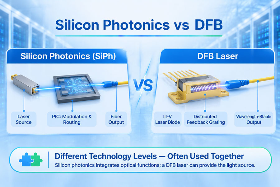
Laser source: Generates the optical carrier used for data transmission. It may be integrated, hybrid-mounted, or supplied externally.
Optical coupling interface: Connects the PIC to optical fibers or other photonic devices.
Package substrate or interposer: Provides mechanical support and electrical routing between components.
Thermal management structure: Controls heat generated by active optical and electronic components.
The purpose is to ensure that all components operate together with suitable optical loss, electrical performance, temperature stability, mechanical reliability, and manufacturing consistency.
2. Why Is Advanced Optical Packaging Becoming More Important?
Higher data rates increase the complexity of optical and electrical integration. In conventional pluggable architectures, electrical signals travel from the switch ASIC through the system board and into the optical module before reaching the optical engine. As signaling speeds increase, these electrical paths become more challenging to design.
Advanced packaging can reduce the distance between electronic and photonic components and provide more controlled optical and electrical connections.
Several factors are driving its development:
Higher bandwidth density: More data must pass through increasingly compact optical engines and switch systems.
Electrical signal integrity: Shorter, better-controlled electrical connections help manage insertion loss, crosstalk, and other high-speed signal impairments.
Power efficiency: Reducing unnecessary electrical channel losses and signal-conditioning requirements can help improve energy efficiency.
Thermal constraints: Dense optical and electronic integration creates localized heat that must be managed carefully.
Photonic integration: Silicon photonics and heterogeneous integration require precise connections between different materials and devices.
Manufacturing scalability: High-volume optical systems need repeatable alignment, assembly, testing, and qualification processes.
These requirements are particularly relevant to AI data centers, where large numbers of accelerators and switches exchange data through high-bandwidth optical networks.
3. Main Technologies Used in Advanced Optical Packaging
Advanced optical packaging combines several technologies. Each addresses a different part of the integration process, from mounting photonic chips to connecting optical fibers and controlling heat.
| Technology | Primary function | Engineering value |
|---|---|---|
| Flip-chip bonding | Mounts semiconductor dies with electrical contacts facing the substrate | Short electrical connections and compact assembly |
| 2.5D integration | Places multiple dies on a common interposer or package substrate | Dense die-to-die routing and flexible component placement |
| 3D integration | Stacks dies vertically using technologies such as TSVs or hybrid bonding | Higher integration density and shorter interconnects |
| Hybrid bonding | Creates fine-pitch electrical and mechanical connections between prepared surfaces | High-density chip-to-chip integration |
| Fiber array attachment | Connects multiple optical fibers to photonic chips | Multi-channel optical coupling |
| Optical micro-optics | Uses lenses, mirrors, and other optical elements to manage light paths | Improved optical alignment and coupling design |
| Thermal interface materials | Transfers heat from active components to cooling structures | Temperature control and operating stability |
These technologies can be combined within one package. For example, a silicon interposer may connect a PIC and an EIC, while a fiber array unit provides the optical connection to external fibers. The final architecture depends on bandwidth, optical interface design, power consumption, and manufacturing requirements.
4. Optical Fiber Coupling and Alignment
Optical coupling is one of the most sensitive aspects of advanced optical packaging. Light must transfer efficiently between the photonic chip and the external optical interface. Small alignment errors can increase insertion loss and reduce the available optical power budget.
Two common coupling approaches are edge coupling and grating coupling.
Edge coupling directs light through the edge of a photonic chip. It often uses a tapered waveguide or spot-size converter to match the optical mode of the chip to the mode of the fiber.
Grating coupling uses a periodic structure on the photonic chip to couple light between the waveguide and a fiber positioned above the chip. It can simplify certain assembly arrangements, although coupling efficiency and wavelength characteristics depend on the grating design.
| Feature | Edge coupling | Grating coupling |
|---|---|---|
| Light interface | Chip edge | Chip surface |
| Fiber arrangement | Typically aligned with the waveguide direction | Often positioned above the chip at a designed angle or orientation |
| Optical design | Uses edge tapers or mode converters | Uses periodic optical structures |
| Packaging considerations | Edge preparation, fiber positioning, and mechanical stability | Grating design, fiber placement, and wavelength dependence |
For multi-channel photonic devices, fiber array units (FAUs) are commonly used to connect multiple fibers to a photonic chip. The fiber pitch, coupling geometry, alignment tolerance, and mechanical attachment method must match the PIC design.
Passive alignment relies on precisely manufactured mechanical reference features to position components. Active alignment uses optical measurements to adjust the relative position of components and identify an acceptable coupling condition. Some production flows combine both approaches: precision is built into component fabrication and bonding, while active alignment corrects remaining placement errors.
5. Electrical Integration Between PIC and EIC
An optical engine typically contains both a photonic integrated circuit and electronic integrated circuits. The PIC handles optical functions, while the EIC provides the electrical drive and receiver circuitry required for high-speed data transmission.
The connection between these chips is a major packaging challenge. High-speed electrical signals are sensitive to parasitic capacitance, inductance, impedance discontinuities, insertion loss, and crosstalk.
Advanced packaging technologies help control these effects through:
Shorter interconnects: Flip-chip and interposer-based layouts can reduce the distance between the driver or receiver electronics and the photonic device.
High-density routing: Fine-pitch connections support more electrical channels within a limited package area.
Controlled impedance: Package traces and interconnect structures are designed to maintain signal integrity at high frequencies.
Power distribution: Power and ground structures must support stable operation of sensitive electronic and photonic components.
Signal isolation: Layout, shielding, and grounding strategies help reduce unwanted coupling between high-speed channels.
The objective is not simply to place chips closer together. The electrical path must also be engineered to meet the required bandwidth and signal-quality targets.
6. Thermal Management in Optical Packaging
Thermal management is essential because optical and electronic components can have different operating-temperature requirements. Lasers, drivers, DSPs, and switch ASICs generate heat, while temperature changes can affect optical wavelength, modulation behavior, and component reliability.
Advanced optical packaging must provide an effective thermal path from heat-generating devices to the cooling system.
Common thermal management approaches include:
Heat spreaders: Distribute heat across a larger surface area to reduce localized temperature concentration.
Thermal interface materials: Improve heat transfer between semiconductor packages and cooling structures.
Heat sinks: Transfer heat from the package to the surrounding airflow or another cooling medium.
Liquid cooling: Supports systems with high heat density when air cooling is insufficient or less efficient for the required design.
Thermal isolation: Separates temperature-sensitive components from nearby heat sources where practical.
Optical fiber attachment also introduces thermal constraints. Temperature changes can cause mechanical expansion or stress at the fiber-to-chip interface, potentially changing alignment and coupling efficiency.
7. Advanced Optical Packaging and CPO, NPO, and OBO
Advanced optical packaging enables several system architectures that move optical engines closer to electronic processing devices. These architectures differ mainly in where the optical engine is positioned relative to the switch ASIC or processor.
| Architecture | Optical engine location | Packaging focus | Main trade-off |
|---|---|---|---|
| Pluggable optics | Removable front-panel module | Compact module assembly and host electrical interface | Longer electrical path, but convenient replacement |
| On-board optics (OBO) | Mounted on the system board | Board-level optical and electrical integration | Closer placement, but board-level servicing and routing constraints |
| Near-packaged optics (NPO) | Near the ASIC or processor package | Short electrical connections and optical access | Greater integration with additional thermal and serviceability considerations |
| Co-packaged optics (CPO) | Integrated within or very close to the main ASIC package | High-density PIC, EIC, fiber, and package integration | Short electrical paths, but demanding assembly and maintenance requirements |
Pluggable optics keep the optical engine in a removable module. This provides flexibility for replacement, upgrades, and different optical reach requirements.
OBO moves optical components onto the system board, reducing some of the distance between the switch and the optical engine. NPO places the optical engine closer to the main ASIC package. CPO integrates optical engines within or immediately adjacent to the ASIC package assembly.
As integration becomes tighter, the package must handle more demanding electrical routing, optical fiber attachment, thermal design, and repair strategies.
Advanced optical packaging is therefore an enabling technology for CPO, but the two terms are not interchangeable. Advanced packaging also applies to conventional pluggable modules, on-board optics, coherent optical engines, and other photonic devices.
8. The Role of Advanced Packaging in 800G and 1.6T Optical Transceivers
800G and 1.6T optical systems place increasing demands on component density, electrical bandwidth, optical coupling, and thermal performance. As more channels are integrated into a limited space, packaging becomes a major factor in achieving stable system operation.
In an optical transceiver, packaging must support several functions at the same time:
Positioning the laser, PIC, receiver, and electronic components accurately.
Maintaining low-loss optical connections between photonic devices and fibers.
Supporting high-speed electrical interfaces between the host and optical engine.
Providing sufficient heat transfer for active components.
Maintaining mechanical stability under operating and environmental conditions.
Allowing consistent production testing and final module qualification.
C-LIGHT's current product portfolio includes several high-speed optical connectivity options:
400G QSFP-DD Optical Transceivers for supported 400G network platforms.
400G OSFP Optical Transceivers for compatible OSFP-based equipment.
800G QSFP-DD Optical Transceivers for supported 800G host interfaces.
800G OSFP Optical Transceivers for high-bandwidth data center connectivity.
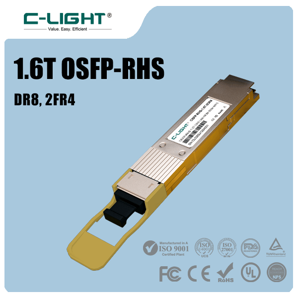
1.6T OSFP-RHS for systems designed to support the corresponding module interface and thermal requirements.
800G AOC and 800G AEC for suitable short-reach interconnect applications.
These products operate within their respective module and cable architectures. Their inclusion does not imply that every model uses CPO or the same internal packaging process. Actual module construction, optical engine design, and thermal characteristics must be confirmed through individual product specifications.
9. Reliability, Testing, and Manufacturing Yield
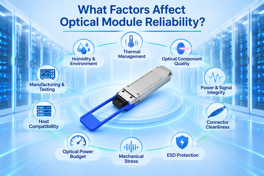
Advanced optical packaging must deliver repeatable performance across production batches and maintain stability throughout the intended operating life. A photonic device that performs well during initial assembly may still experience problems caused by thermal cycling, mechanical stress, contamination, or long-term alignment changes.
Important qualification areas include:
Optical insertion loss: Measures the optical power lost through the packaged optical path.
Coupling stability: Evaluates whether fiber-to-chip alignment remains consistent during operation and environmental testing.
Electrical performance: Checks high-speed signal integrity, impedance behavior, and electrical interface characteristics.
Thermal cycling: Evaluates the impact of temperature changes on materials, bonds, and optical alignment.
Mechanical reliability: Tests the package's resistance to vibration, handling, and other relevant mechanical conditions.
Environmental protection: Assesses the effects of humidity, contamination, and other operating conditions.
Production yield: Measures the proportion of assemblies that meet all required specifications.
Testing can take place at several stages, including wafer-level photonic testing, die-level testing, package-level optical testing, and final system qualification. Earlier testing can help identify defects before expensive assembly stages are completed.
For high-volume manufacturing, process control is especially important. Precision bonding, fiber placement, optical inspection, automated testing, and statistical process monitoring all contribute to consistent production quality.
10. Key Challenges in Advanced Optical Packaging
Although advanced packaging enables higher integration density, it also introduces new engineering and manufacturing difficulties.
Precision alignment: Optical coupling structures may require extremely accurate positioning. Small variations can produce measurable changes in insertion loss.
Thermal interaction: The close placement of electronic and photonic devices creates temperature gradients that can affect optical behavior and mechanical stability.
Packaging complexity: Combining PICs, EICs, interposers, fiber arrays, and cooling structures increases the number of interfaces that must be designed and controlled.
Manufacturing yield: A defect in one optical or electrical interface can affect the performance of the complete assembly. Rework may become difficult as integration density increases.
Repairability: Pluggable modules can generally be replaced independently. Tightly integrated optical engines may require more complex maintenance or package-level replacement strategies.
Standardization: Optical interfaces, fiber attachment, electrical connections, management, and thermal requirements must be sufficiently defined to support reliable manufacturing and interoperability.
Cost and supply chain: Advanced substrates, precision bonding equipment, optical testing, and specialized packaging processes can increase manufacturing investment and create supply-chain dependencies.
11. Future Trends in Advanced Optical Packaging
The next stage of optical packaging development will be shaped by the increasing integration of photonic and electronic components. AI computing, high-capacity switching, and future optical interconnects are driving demand for more compact and efficient optical engines.
Several technology directions are particularly important:
Co-packaged optics: Closer integration of optical engines and high-performance ASICs to reduce electrical interconnect distance.
Hybrid bonding: Finer-pitch connections between electronic and photonic components for denser package architectures.
Advanced interposers: Silicon, glass, and other interposer technologies for high-density electrical and optical integration.
3D photonic integration: Vertical stacking and advanced chiplet arrangements to increase integration density.
Automated optical assembly: More precise and repeatable fiber placement, bonding, and inspection processes.
Improved thermal solutions: Advanced heat spreaders, thermal interface materials, and liquid-cooling-compatible package designs.
Optical I/O: Photonic interfaces positioned closer to processors and accelerators for future high-bandwidth systems.
These developments will not necessarily replace pluggable optical modules across all applications. Different architectures will coexist because data center links, accelerator connections, campus networks, and long-distance optical systems have different requirements for reach, serviceability, cost, and bandwidth density.
12. Conclusion
Advanced optical packaging is a critical enabling technology for modern optical communication. It connects photonic integrated circuits, electronic components, laser sources, and optical fibers into reliable assemblies while managing signal integrity, optical coupling, heat dissipation, and mechanical stability.
As optical connectivity progresses through 800G and 1.6T toward higher-capacity systems, packaging quality will increasingly influence the performance and commercial viability of optical engines. Technologies such as flip-chip bonding, hybrid bonding, interposers, fiber array attachment, and advanced thermal management will support denser photonic integration.
Advanced optical packaging also provides the manufacturing foundation for emerging NPO, CPO, and optical I/O architectures. Its long-term success will depend on precision assembly, repeatable production processes, reliability qualification, and practical maintenance strategies.
For current high-speed optical connectivity requirements, visit the C-LIGHT Optical Transceiver portfolio or Contact C-LIGHT for product and technical information.
 >

 >
 >
 >
 >
 >
 >
 >