TEL:+86 132 6656 7067





As artificial intelligence workloads expand, data movement between GPUs, accelerators, memory systems and network switches is becoming a major infrastructure challenge. Optical chips are gaining importance because they enable high-capacity communication through light, helping AI systems scale beyond the limits of conventional electrical interconnects.
Why AI Infrastructure Needs Optical Chips
Large AI training and inference systems rely on many accelerators operating together. In distributed training, GPUs exchange model gradients, intermediate results and synchronization data across high-speed networks. As clusters grow, communication performance can directly affect accelerator utilization and overall computing efficiency.
Electrical interconnects remain effective for many short-distance connections, but increasing data rates create challenges involving insertion loss, signal integrity, equalization and power consumption. These constraints become more significant when large numbers of high-speed links must fit within limited rack and package space.
Optical chips help address these challenges by converting electrical data into optical signals, manipulating light through integrated photonic components, or supporting optical input/output close to computing and switching devices. Their value extends beyond transmission speed to bandwidth density, reach, power management and system scalability.
What Is an Optical Chip?
An optical chip integrates photonic functions onto a semiconductor platform. Depending on its design, it may guide light, modulate optical signals, combine or separate wavelengths, detect incoming light, or support optical signal processing.
Silicon photonics is one important implementation approach. It uses silicon-based photonic structures alongside electronic control and signal-processing circuits. Because silicon photonics can use manufacturing techniques derived from established semiconductor processes, it offers a pathway toward denser integration and scalable production. However, lasers, coupling structures, packaging and electronic interfaces may still require additional components or specialized processes.
Optical Modulators
Convert electrical data into changes in an optical carrier, enabling information to be transmitted through fiber.
Photodetectors
Convert received optical signals back into electrical signals for downstream processing.
Waveguides and Multiplexers
Guide light across a chip and combine or separate wavelength channels to support optical transmission.
Optical Engines
Integrate multiple photonic components with associated electronics to provide optical transmit and receive functions.
How Optical Chips Support AI Data Centers
Optical chips can contribute at several layers of AI infrastructure. Their role depends on the system architecture, required reach, link speed, thermal conditions and serviceability requirements.
| Application | Role of Optical Chips | Infrastructure Benefit |
|---|---|---|
| GPU cluster networking | Support high-speed optical links between network interfaces and switches. | Higher aggregate bandwidth for distributed training and inference traffic. |
| Switch-to-switch links | Enable dense optical connections across racks and network tiers. | Improved reach and bandwidth density for scale-out fabrics. |
| Near-package optical I/O | Place optical engines close to high-speed ASICs to shorten electrical paths. | Potential reductions in electrical loss and interface power. |
| Co-packaged optics | Integrate optical engines near or within a switch package architecture. | Potentially greater front-panel bandwidth density and improved electrical-interface efficiency. |
| Emerging photonic computing | Use optical devices to accelerate selected computational or signal-processing operations. | Potential benefits for specialized workloads, subject to system-level efficiency and scalability. |
Silicon Photonics and Optical Interconnect Evolution
Silicon photonics is increasingly relevant as AI infrastructure moves toward higher aggregate bandwidth and tighter integration. Rather than treating optics only as a pluggable module at the front panel of a switch, system designers are evaluating how optical functions can be positioned closer to the switching or computing silicon.
Several approaches coexist, each with different implications for power, packaging, maintenance and deployment.
| Technology | Architecture | Potential Advantages | Key Considerations |
|---|---|---|---|
| Pluggable optical transceivers | Optical modules connect through host electrical interfaces and removable cages. | Established deployment model, field replaceability and flexible reach options. | High-speed electrical paths between the host ASIC and module can consume power and constrain signal integrity. |
| Linear-drive pluggable optics (LPO) | Reduces or removes some module-side retiming and DSP functions, depending on implementation. | Can lower power consumption and simplify the signal chain. | Requires careful host-channel design, signal integrity management and interoperability validation. |
| Near-packaged optics (NPO) | Positions optical engines close to the host ASIC package. | Shorter electrical connections and potential improvements in bandwidth density. | Packaging, thermal design, optical connections and service procedures become more complex. |
| Co-packaged optics (CPO) | Integrates optical engines alongside or within the switch ASIC package architecture. | Potentially reduces high-speed electrical interconnect distance and supports very high aggregate bandwidth. | Raises requirements for thermal management, reliability, manufacturing yield and field maintenance. |
These technologies are not direct replacements for one another in every deployment. Pluggable optics remain useful where flexibility and serviceability are priorities, while NPO and CPO target architectures that need tighter integration and higher bandwidth density.
Bandwidth, Power and Thermal Efficiency
AI infrastructure performance depends on more than the nominal data rate of a link. Designers must consider the power consumed by the complete transmission path, including the host ASIC interface, driver, modulator, laser source, photodetector, receiver electronics and any required digital signal processing.
Optical chips can help reduce some electrical transmission constraints, especially when optical conversion occurs close to the source of the data. However, the total benefit depends on the implementation. Optical conversion itself consumes energy, and laser operation, coupling losses, thermal control and signal conditioning remain part of the system budget.
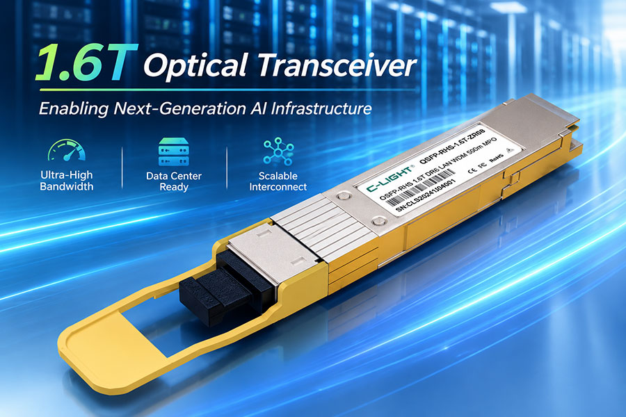
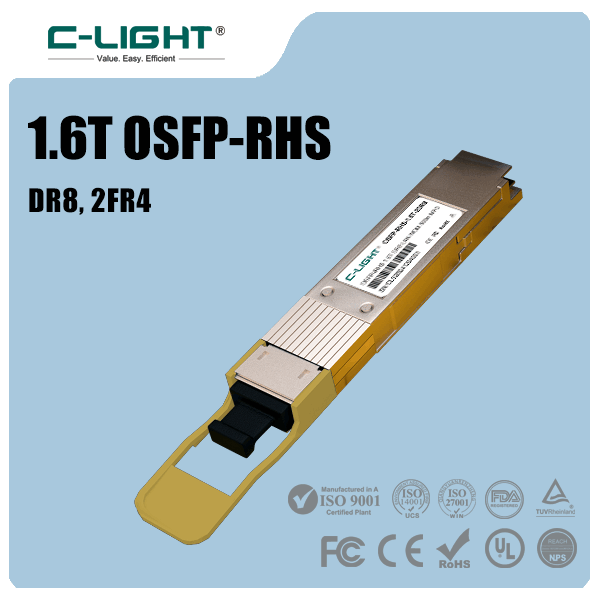
As network speeds advance through 400G, 800G and emerging 1.6T-class interconnects, implementations may use different lane counts, modulation formats, wavelengths and packaging arrangements. The practical objective is to deliver the required bandwidth while balancing energy per bit, reach, reliability and cost.
Optical Chips Versus Photonic AI Accelerators
Optical communication and photonic computing are related but distinct fields. Communication-focused optical chips carry data between components. Photonic AI accelerators attempt to use light to execute selected operations, such as certain matrix computations or optical signal-processing tasks.
| Comparison | Optical Communication Chips | Photonic AI Accelerators |
|---|---|---|
| Primary purpose | Transmit and receive data across optical links. | Perform selected computations using photonic mechanisms. |
| Typical functions | Modulation, detection, wavelength routing and optical I/O. | Optical matrix operations or specialized signal processing. |
| Integration target | Transceivers, optical engines, switches and compute packages. | Specialized accelerator systems or heterogeneous computing platforms. |
| Main challenges | Power, optical coupling, packaging, reliability and link interoperability. | Data conversion overhead, precision, programmability, scalability and software integration. |
For near-term AI infrastructure planning, optical interconnects are a practical focus because they address the established need to move large volumes of data between distributed compute resources. Photonic computing remains an additional area of development, with its usefulness depending on workload characteristics and complete system performance.
Engineering Challenges and Deployment Considerations
The adoption of optical chips requires coordinated engineering across photonics, electronics, packaging and network architecture. A photonic device with strong laboratory performance does not automatically deliver the same benefit in a deployed AI cluster.
Thermal management: Lasers, electronic drivers, switches and accelerators generate heat in densely packed systems. Temperature variation can affect optical performance and component lifetime.
Packaging and optical coupling: Aligning photonic devices with fibers, lasers and electronic components requires reliable assembly processes and controlled tolerances.
Manufacturing yield: Integrated photonic devices and advanced packages must meet consistent performance targets at production scale.
Testing and reliability: Optical power, receiver sensitivity, bit error rate, temperature behavior and interoperability need to be validated across operating conditions.
System-level power: Comparisons should include the full electrical and optical path rather than measuring the photonic chip in isolation.
Maintainability: Tightly integrated optical engines can complicate replacement and repair, making reliability and service strategy important design factors.
What This Means for AI Network Design
Optical chips are becoming a strategic building block for AI infrastructure, but choosing a solution requires more than selecting the highest available bandwidth. Network architects should evaluate link distance, topology, port density, power limits, fiber plant, cooling capability and expected growth.
For many deployments, pluggable transceivers provide a flexible way to scale high-speed links. For systems facing tighter electrical-interface constraints, LPO, NPO or CPO may offer alternatives, provided the associated host design, thermal requirements, reliability targets and maintenance model are suitable.
Optical technology also works alongside network software, congestion control and topology design. Faster optical links cannot independently eliminate every communication bottleneck, so infrastructure planning should consider the entire data path from accelerator interfaces through switches and optical links.
Frequently Asked Questions
1. What are optical chips used for in AI infrastructure?
They support optical data transmission, signal conversion and optical I/O between accelerators, switches and other high-speed computing components. Some emerging photonic chips are also designed to perform specialized computational operations.
2. What is the role of silicon photonics in AI data centers?
Silicon photonics integrates optical functions on a semiconductor platform, supporting compact optical engines and high-bandwidth interconnects. Its benefits depend on the electronic interfaces, laser source, packaging and system architecture.
3. Will optical chips replace copper connections?
Not universally. Copper remains practical for many short-reach connections, while optical links are increasingly valuable when bandwidth, distance, signal integrity or electrical power constraints make them a better fit.
4. How do CPO and NPO differ from pluggable optics?
Pluggable optics use removable modules connected through host electrical interfaces. NPO places optical engines close to the host ASIC, while CPO integrates optical engines within the ASIC package architecture or immediately alongside it. These approaches trade serviceability and design flexibility against potential gains in integration and bandwidth density.
5. Do optical chips automatically reduce AI data center power consumption?
No. They can reduce certain electrical transmission and signal-conditioning costs, but lasers, optical conversion, drivers, receivers, cooling and packaging also consume power. System-level measurements are needed to establish the actual benefit.
6. What should engineers evaluate when selecting optical interconnects?
Important factors include data rate, transmission distance, optical budget, connector and fiber type, power consumption, host compatibility, thermal conditions, interoperability and long-term serviceability.
Conclusion
Optical chips are becoming increasingly important as AI infrastructure demands higher bandwidth, greater interconnect density and more efficient data movement. Silicon photonics, optical engines, NPO and CPO provide different paths toward tighter integration between computing and optical communication.
The most effective design depends on the complete system rather than a single component. Matching optical technology to link distance, network architecture, power limits and maintenance requirements will be essential as AI clusters continue to scale.
Planning high-speed optical connectivity for AI or data center networks?
Discuss optical transceiver options, link requirements and compatibility considerations with our team.
Contact C-LIGHT >

 >
 >
 >
 >
 >
 >
 >