TEL:+86 132 6656 7067





Next-generation AI data centers require higher bandwidth per optical link without unlimited increases in port count, power consumption or cooling demand. Silicon photonics offers a path toward highly integrated 1.6T optical engines by combining waveguides, modulators and wavelength-routing functions on photonic integrated circuits (PICs).
At 1.6 terabits per second, the challenge extends beyond increasing optical bandwidth. High-speed electrical signaling, laser integration, optical coupling, receiver performance and thermal control must work together within a compact module or system package. Silicon photonics can support this integration, but its benefits depend on the complete transceiver architecture and manufacturing process.
1. Why Silicon Photonics Matters at 1.6T
A nominal 1.6T link doubles the aggregate line rate of an 800G link. Depending on the implementation, that increase can come from higher per-lane signaling rates, more optical lanes or a combination of both. Each approach creates different demands on the electrical interface, optical engine and fiber connection.
Silicon photonics helps integrate multiple optical functions into a compact area. This can be particularly useful when a transceiver must accommodate several high-speed channels, wavelength multiplexing and precise optical routing while meeting strict mechanical and thermal limits.
2. How a Silicon Photonics 1.6T Transceiver Works
A typical pluggable optical transceiver receives high-speed electrical data from a switch ASIC, processes the signals as required, converts them into optical channels and transmits them through fiber. The receiving endpoint performs optical-to-electrical conversion and reconstructs the incoming data.
Simplified transmit path. The receive path uses photodetection and receiver electronics. Actual DSP placement, lane count and optical architecture vary by implementation.
The laser supplies the optical carrier. Modulators encode the electrical data onto the light, and silicon waveguides route the optical signals. When the design uses wavelength-division multiplexing (WDM), integrated or hybrid optical components combine multiple wavelengths for transmission through fewer fiber strands.
At the receiving end, photodetectors convert light into electrical signals. Receiver circuitry amplifies and conditions those signals, while DSP and forward error correction (FEC) may be used according to the relevant interface specification.
3. 200G-Class Lanes and High-Speed Signal Integrity
Many 1.6T transceiver designs target 200G-class electrical or optical lanes. Such architectures can increase aggregate bandwidth without proportionally increasing the number of channels, but they impose demanding requirements on bandwidth, noise, jitter and channel loss.
PAM4 signaling is important in many high-speed optical implementations because it carries two bits per symbol. However, the actual modulation format, lane count, baud rate and FEC requirements must be confirmed from the relevant interface specification. The 1.6T aggregate rate alone does not uniquely determine these parameters.
| Design Element | Primary Challenge | Effect on 1.6T Performance |
|---|---|---|
| Electrical host channel | Insertion loss, crosstalk and jitter | Can limit signal quality between the switch ASIC and optical engine |
| Modulator | Bandwidth, drive voltage and optical loss | Affects transmitter power, signal quality and reach |
| Laser source | Optical output, wavelength stability and efficiency | Determines available optical power and thermal requirements |
| Photodetector and receiver | Bandwidth, responsivity and noise | Influences sensitivity and bit-error performance |
| DSP and FEC | Signal recovery, power and processing latency | Helps maintain link performance under the specified channel conditions |
Silicon photonics does not eliminate electrical signal-integrity challenges. The PIC must still interface with high-speed electronic circuitry, and the complete package must maintain the required electrical and optical performance across operating conditions.
4. Photonic Integrated Circuits and Optical Functions
The photonic integrated circuit is the core of a silicon photonics design. It guides light through patterned waveguides and can integrate multiple optical functions that would otherwise require separate components.
| PIC Function | Purpose | Key Engineering Parameter |
|---|---|---|
| Waveguides | Route light between optical components | Propagation loss, bend loss and coupling efficiency |
| Modulators | Encode electrical data onto an optical carrier | Bandwidth, insertion loss, drive voltage and linearity |
| Wavelength multiplexers | Combine separate wavelengths onto a common path | Channel isolation, insertion loss and wavelength alignment |
| Wavelength demultiplexers | Separate incoming wavelengths into individual channels | Channel spacing, isolation and thermal sensitivity |
| Optical splitters and couplers | Distribute or transfer optical power between paths | Excess loss, uniformity and alignment tolerance |
| Monitoring structures | Support optical power monitoring or control | Measurement accuracy and integration overhead |
Not every PIC contains all these functions, and not every function is implemented exclusively in silicon. Laser sources, semiconductor optical amplifiers and certain detectors may use other materials or hybrid integration techniques. The specific material stack depends on the optical function and the manufacturer's process.
5. Laser Integration and Wavelength Management
Silicon is effective for guiding and manipulating light but is not normally used as a conventional light-generating laser material. Silicon photonics transceivers therefore commonly rely on external laser sources or hybrid integration with suitable compound-semiconductor devices.
At 1.6T, laser integration must deliver the required optical power and wavelength stability while minimizing coupling loss and thermal overhead. In wavelength-multiplexed designs, channel alignment and temperature behavior are especially important because optical filters and multiplexers operate within defined wavelength ranges.
Engineers must consider:
Laser output power and efficiency at the intended operating temperature.
Wavelength stability and compatibility with the optical channel plan.
Coupling loss between the laser, PIC and fiber interface.
Thermal interaction between the laser, modulator and surrounding electronics.
Redundancy, monitoring and serviceability requirements where applicable.
Whether a laser is external, hybrid-integrated or packaged in another arrangement depends on the module design. Silicon photonics should not be assumed to mean that the laser is fabricated directly on the silicon PIC.
6. Parallel Optics and Wavelength-Multiplexed Architectures
1.6T optical interconnects can use parallel optical lanes or multiple wavelengths carried over fewer fiber strands. Silicon photonics can support both approaches, although the actual design depends on the applicable optical interface and product architecture.
| Characteristic | Parallel Optics | Wavelength-Multiplexed Optics |
|---|---|---|
| Transmission method | Multiple optical paths carry separate lanes | Multiple wavelengths share an optical path |
| Fiber infrastructure | May require multiple fibers per direction | Can reduce fiber-strand requirements |
| PIC requirements | Multiple modulators and optical paths may be integrated | Wavelength multiplexing and demultiplexing functions are important |
| Primary trade-off | Fiber count, connector mapping and parallel-lane management | Wavelength control, filter loss and channel isolation |
| Deployment priority | Validate lane mapping, connector polarity and channel loss | Validate wavelength plan, fiber interface and optical budget |
These approaches are not interchangeable at the cabling level. The correct fiber count, connector type, polarity and reach depend on the transceiver's defined optical interface. A module using a compact PIC may still require a multi-fiber connector, while another design may support a duplex-fiber connection through wavelength multiplexing.
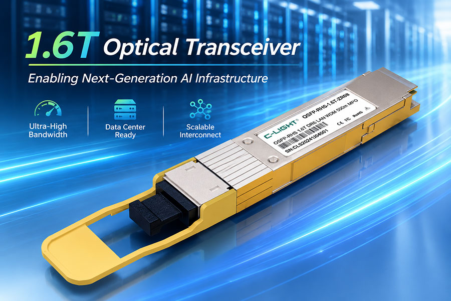
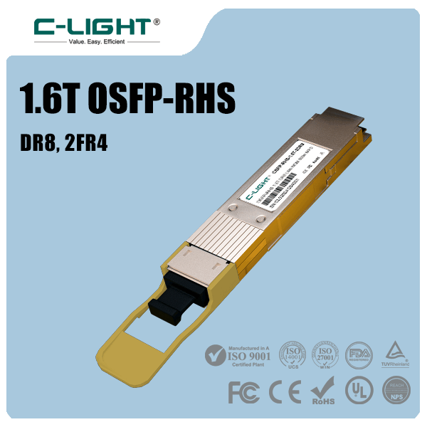
7. 1.6T OSFP and OSFP-RHS Integration
High-speed pluggable transceivers must fit the mechanical, electrical and thermal constraints of their host platforms. OSFP-family form factors are relevant to high-capacity data center systems, while OSFP-RHS refers to a reduced-height configuration used in particular platform designs.
Silicon photonics can be used within different module form factors. The form factor itself does not specify the PIC architecture, optical reach, wavelength plan or laser implementation.
| Integration Area | What Must Be Validated |
|---|---|
| Mechanical interface | Cage dimensions, connector alignment and host-platform support |
| Electrical interface | Lane rate, signal integrity and supported host configuration |
| Power delivery | Module power class and switch-port power limits |
| Thermal design | Airflow direction, case-temperature range and cooling capability |
| Serviceability | Module access, fiber routing and replacement procedures |
Mechanical fit alone does not establish compatibility. Before deployment, confirm that the switch supports the exact transceiver type, firmware behavior, electrical interface and thermal requirements.
8. Power Efficiency and Thermal Management
Higher bandwidth per port can improve network capacity density, but 1.6T modules operate within a demanding power and cooling envelope. Silicon photonics may improve integration efficiency, yet total power also depends on the DSP, driver, receiver, laser and any wavelength-control circuitry.
Energy-efficiency comparisons should use a consistent system boundary. Module power, optical-engine power and total switch power are different measurements. A design with a smaller PIC is not necessarily more efficient if it requires more electronic processing or thermal control.
| Factor | Potential Impact | Evaluation Approach |
|---|---|---|
| Optical integration | Can reduce discrete-component count and routing complexity | Evaluate complete module power and manufacturing results |
| DSP and drivers | Can account for a significant share of transceiver power | Measure power at the required signaling rate and operating mode |
| Laser efficiency | Influences electrical input power and thermal load | Review output power, efficiency and temperature performance |
| Wavelength control | May add control circuitry and thermal overhead | Check stabilization requirements under operating conditions |
| System cooling | Determines whether dense port populations can operate reliably | Validate chassis airflow, module limits and rack-level cooling |
Liquid cooling may support higher system-level thermal density, but it does not necessarily cool each optical engine directly. Actual results depend on the host chassis, heat-transfer path and the module's specified operating limits.
9. Silicon Photonics Versus InP for 1.6T
Silicon photonics and indium phosphide (InP) photonics offer different strengths. Silicon photonics is well suited to dense waveguide integration and optical routing, while InP supports light generation and can integrate several active optical functions. Some transceiver architectures combine materials to use the strengths of each platform.
| Comparison Area | Silicon Photonics | InP-Based Photonics |
|---|---|---|
| Waveguide integration | Compact, high-index-contrast silicon waveguides | Supports integrated optical paths using compound-semiconductor processes |
| Laser implementation | Often uses external or hybrid-integrated laser sources | Can integrate laser functions within the photonic platform |
| Manufacturing approach | Can leverage silicon wafer processing, with specialized photonics steps | Uses compound-semiconductor fabrication processes |
| Integration trade-offs | Laser coupling, optical loss and thermal control require careful design | Process cost, integration density and device-specific constraints vary |
| Best-fit decision | Depends on required integration, optical performance and volume | Depends on required active-device integration and performance targets |
Neither technology is universally better for every 1.6T transceiver. A meaningful comparison should include link performance, power, temperature stability, packaging, manufacturing yield, reliability and cost at the intended production volume.
10. From 1.6T Pluggable Optics to Co-Packaged Optics
As electrical lane rates rise, the distance between the switch ASIC and optical engine becomes increasingly important. Co-packaged optics (CPO) places optical engines close to the switch ASIC, potentially reducing the length and power demands of high-speed electrical connections.
Silicon photonics is a potential enabling technology for CPO because it can integrate multiple optical functions in a compact footprint. However, the two concepts describe different layers of the design: silicon photonics concerns photonic integration, while CPO concerns how optical engines are packaged within the system.
Pluggable 1.6T transceivers and CPO also present different operational trade-offs. Pluggable modules offer a familiar replacement model, while CPO changes the location of optical connections and can introduce more demanding fiber attachment and service procedures. Selection depends on platform design, maintainability, thermal constraints and deployment scale.
11. Frequently Asked Questions
11.1 Does every 1.6T optical transceiver use silicon photonics?
No. Silicon photonics is one possible integration platform. Other implementations may use InP-based devices or hybrid architectures. The exact technology depends on the transceiver design and product specification.
11.2 Why is silicon photonics useful for 1.6T?
It can integrate multiple optical functions in a compact PIC, helping support dense optical channels and wavelength routing. The final benefit depends on optical loss, electronic power, packaging and thermal performance.
11.3 Does silicon photonics generate its own laser light?
Conventional silicon photonics generally uses an external or hybrid-integrated laser source because silicon is not an efficient conventional laser material. The laser arrangement depends on the specific transceiver architecture.
11.4 Does 1.6T necessarily mean eight 200G optical lanes?
No. Some designs target 200G-class lanes, but aggregate rate alone does not define the number of lanes or the electrical and optical architecture. Confirm the lane configuration in the relevant product specification.
11.5 Is silicon photonics always more power-efficient than InP?
No. Power efficiency depends on the complete transmitter and receiver, including the laser, drivers, DSP, thermal controls and packaging. The material platform alone is insufficient to determine total power.
11.6 Can a silicon photonics 1.6T module operate in any OSFP switch?
No. The exact host interface, form factor, power limits, thermal requirements, firmware and optical configuration must be supported by the switch. A matching connector does not guarantee operational compatibility.
12. Conclusion
Silicon photonics can play a significant role in 1.6T optical transceivers by integrating modulators, waveguides and wavelength-routing functions into compact photonic circuits. At this bandwidth, however, the PIC is only one part of a demanding design that also includes high-speed electronics, laser integration, fiber coupling, packaging and thermal management.
For AI data center deployments, the most effective 1.6T solution is the one that meets the required link rate and reach while maintaining validated host compatibility, acceptable power consumption and reliable operation. Silicon photonics provides important integration capabilities, but system-level performance and manufacturability determine its practical value.
Share your target bandwidth, switch platform, transmission distance, fiber interface and thermal requirements to evaluate suitable high-speed transceiver options.
Contact C-LIGHT >

 >
 >
 >
 >
 >
 >
 >