TEL:+86 132 6656 7067





Silicon photonics enables multiple optical functions to be integrated into a compact photonic integrated circuit (PIC), but the chip is only one part of a complete optical transceiver. Packaging must connect the PIC to optical fibers, laser sources, high-speed electronic components and the external thermal environment while preserving optical performance and long-term reliability.
As data center links move toward 800G and 1.6T, packaging becomes increasingly important. Higher aggregate bandwidth, tighter power budgets, more demanding electrical interfaces and denser optical integration leave less room for losses and manufacturing variation. A photonic circuit that performs well at wafer level may still encounter significant challenges after assembly into a transceiver or optical engine.
1. Why Silicon Photonics Packaging Is Difficult
These challenges interact. For example, a package redesign that shortens electrical paths may change the thermal layout, while a fiber-coupling solution that reduces insertion loss may require more precise assembly. Packaging therefore needs to be designed alongside the PIC, laser, electronic integrated circuits and host interface—not added as a final mechanical step.
2. Fiber-to-Chip Optical Coupling Loss
One of the main packaging challenges is transferring light efficiently between the photonic integrated circuit and an optical fiber. Silicon waveguides confine light in a small optical mode, whereas standard fiber has a much larger mode field. Differences in mode size, position, angle and polarization can cause coupling loss.
Edge Coupling
Edge coupling directs light through the side of the PIC, often using inverse-taper structures to expand the optical mode near the chip facet. It can provide low insertion loss and broad optical bandwidth, but requires accurate alignment between the fiber or optical assembly and the chip edge. Facet quality and package geometry also affect repeatability.
Grating Coupling
Grating couplers transfer light through a patterned structure at the chip surface. They can simplify wafer-level testing and support top-side optical access. Their performance depends on wavelength, polarization, fiber angle and grating geometry. The coupling bandwidth and insertion loss may differ from those of a well-designed edge-coupled interface.
| Coupling Method | Advantages | Packaging Challenges |
|---|---|---|
| Edge coupling | Potentially low loss and broad optical bandwidth. | Requires precise lateral, vertical and angular alignment; chip-facet quality is important. |
| Grating coupling | Convenient surface access and useful for wafer-level optical testing. | Can be more sensitive to wavelength, polarization and incidence angle. |
| Lens-assisted coupling | Can help match optical modes and accommodate selected package geometries. | Adds optical components, alignment steps and potential mechanical sensitivity. |
Coupling performance should be evaluated across the intended wavelength range and operating conditions. A low-loss result obtained during initial alignment is not sufficient if adhesive curing, temperature changes or mechanical stress shift the optical interface after assembly.
3. Precision Alignment and Assembly Tolerances
Optical coupling can be highly sensitive to small positional errors. The allowable tolerance depends on the waveguide design, mode-field size, coupling structure and target loss. A package must maintain the required alignment throughout attachment, curing, handling and operation.
Active alignment: Optical power or another live measurement guides component positioning. This can achieve high coupling efficiency but may increase assembly time and equipment cost.
Passive alignment: Mechanical reference features and accurately fabricated structures establish component positions. This supports scalable assembly but depends on the combined tolerance of the die, fiber array and package.
Adhesive control: Adhesive flow, shrinkage and curing conditions can move optical components or introduce stress.
Fiber-array positioning: Channel pitch, end-face quality and angular alignment must match the PIC interface, especially for parallel optical connections.
Inspection and calibration: Automated measurement helps identify coupling errors and maintain consistency between assembly lots.
For multi-channel PICs, alignment complexity grows because several optical paths must meet their loss targets simultaneously. The assembly process must account for channel-to-channel variation rather than optimizing only the strongest optical path.
4. Laser Integration and Optical Source Management
Silicon photonics does not generally provide an efficient native laser source for common telecom wavelengths. A transceiver therefore often uses a separately fabricated laser, an external laser source or a hybrid integration method. The selected architecture affects optical routing, package dimensions, thermal design, serviceability and manufacturing complexity.
| Laser Architecture | Packaging Benefits | Key Trade-Offs |
|---|---|---|
| External laser source | Separates the laser from the photonic chip and can simplify source replacement or thermal isolation. | Requires an optical connection between the source and PIC, adding interface loss and system-level integration requirements. |
| Hybrid integration | Places separately fabricated laser and photonic components in a closely integrated package. | Requires precise assembly, optical alignment and careful management of interfaces. |
| Heterogeneous integration | Integrates dissimilar materials or active devices with the photonic platform. | Requires compatible bonding or integration processes and additional process control. |
Laser integration must account for output power, wavelength stability, optical feedback, coupling loss and heat dissipation. The laser and PIC may have different preferred operating temperatures, so package-level thermal paths and control strategies can affect overall performance.
5. Thermal Management and Wavelength Stability
Heat is generated by lasers, modulators, drivers, TIAs, control electronics and other components. The package must conduct this heat away while keeping temperature-sensitive optical elements within their specified operating range. Higher port density and aggregate data rates can make thermal design more difficult, particularly in compact pluggable modules.
Temperature can affect laser wavelength, refractive index, resonant filters, modulator characteristics and electronic behavior. Resonance-based devices may require especially careful temperature control because a wavelength shift can change the alignment between an optical channel and a filter passband. Other architectures may be less sensitive to resonance shifts but still need stable laser and receiver operation.
Thermal Design Considerations
Provide low-resistance heat paths from high-power electronic and optical components to the package or module housing.
Consider the different thermal requirements of the laser, PIC and electronic integrated circuits.
Reduce unwanted heat transfer into wavelength-sensitive components where practical.
Evaluate temperature gradients, not only the average package temperature.
Validate performance across the specified operating range and under realistic airflow or cooling conditions.
6. High-Speed Electrical Interconnects
Silicon photonics must operate with electronic circuits that drive optical modulators and recover electrical signals from photodetectors. At high lane rates, package traces, bumps, wire bonds, connectors and transitions can introduce impedance discontinuities, parasitic capacitance, inductance and insertion loss.
These effects can reduce electrical bandwidth, degrade signal integrity and increase the burden on equalization or digital signal processing. The package must be treated as part of the high-speed channel rather than as an electrically neutral connection between chips.
| Electrical Challenge | Potential Consequence | Design Response |
|---|---|---|
| Impedance discontinuities | Reflections and waveform distortion. | Control impedance through traces, transitions and package interfaces. |
| Parasitic capacitance and inductance | Reduced bandwidth and degraded signal quality. | Shorten critical connections and optimize interconnect geometry. |
| Long electrical paths | Higher channel loss and greater equalization demands. | Place drivers and receivers close to the photonic devices where practical. |
| Electrical crosstalk | Noise coupling between high-speed lanes. | Optimize routing, spacing, grounding and return paths. |
| Power delivery noise | Jitter or operating-point variation in sensitive circuits. | Design power distribution and decoupling for the complete assembly. |
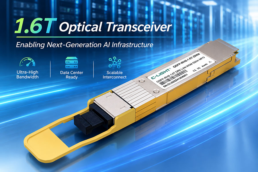
Package design becomes especially important for 800G and 1.6T optical engines, where the aggregate rate is distributed across multiple high-speed electrical and optical lanes. The actual lane rate and interface arrangement depend on the module architecture and implementation.
7. Packaging for 800G and 1.6T Optical Transceivers
Higher-capacity optical modules increase the number of signals and optical channels that must be routed within a constrained volume. Packaging must balance optical access, electrical connectivity, cooling, mechanical strength and manufacturing yield.
For 800G and 1.6T designs, the main engineering pressures include:
Higher aggregate bandwidth: Electrical and optical interfaces must maintain adequate margin at the required lane rates.
Higher connection density: Fiber arrays, electrical routing and component placement compete for limited package area.
Power and thermal limits: Dense integration can create localized hot spots and reduce cooling margin.
Manufacturing repeatability: Small variations in coupling loss, electrical parasitics or thermal behavior can affect final test results.
Serviceability and field handling: The package must withstand installation, removal and handling requirements appropriate to its form factor.
OSFP, QSFP-DD and other module form factors impose different mechanical and thermal constraints. Silicon photonics does not dictate one package type; the final choice depends on port density, host electrical interface, reach, power budget, cooling strategy and system design.
8. Pluggable Optics Versus Co-Packaged Optics
Packaging requirements differ between pluggable optical transceivers and co-packaged optics (CPO). Pluggable modules place the optical engine in a removable module connected to the host through an electrical interface. CPO places optical engines closer to a switch or other high-bandwidth processing ASIC to reduce the length of high-speed electrical connections.
| Consideration | Pluggable Optical Transceivers | Co-Packaged Optics |
|---|---|---|
| Optical engine location | Inside a removable module at the equipment front panel or designated interface. | Near or within the package ecosystem of the host ASIC. |
| Electrical path | Includes the host board and module electrical interface. | Can shorten the high-speed electrical path between the ASIC and optical engine. |
| Optical connection | Fibers connect to the module's external optical ports. | Fiber routing and optical access must be integrated into the system packaging. |
| Maintenance | Modules can generally be replaced independently of the host ASIC. | Serviceability and replacement may be more complex and depend on system architecture. |
| Thermal design | Module cooling must fit the transceiver cage and system airflow. | Must coordinate optical-engine cooling with the ASIC package and surrounding system. |
CPO can reduce electrical interconnect distance, but it does not eliminate optical packaging challenges. Fiber attachment, laser delivery, thermal isolation, reliability and serviceability remain major design considerations. Its suitability depends on the network architecture and operational requirements.
9. Reliability, Qualification and Production Yield
Packaging introduces interfaces between materials with different coefficients of thermal expansion, mechanical properties and moisture sensitivity. Temperature cycling, vibration, humidity, adhesive aging and repeated handling can affect fiber alignment, bonds and electrical connections over time.
Qualification should be tailored to the intended product and operating environment. Common evaluation areas include:
Optical insertion loss and channel uniformity before and after environmental stress.
Laser output and wavelength behavior across specified operating temperatures.
High-speed electrical performance and error-rate measurements after assembly.
Mechanical integrity of fiber attachments, bonds and package interfaces.
Thermal performance under realistic operating power and cooling conditions.
Manufacturing traceability for optical alignment, assembly settings and final test results.
Yield optimization requires measurement at multiple stages. Wafer-level tests screen the PIC, intermediate assembly tests identify coupling or interconnect problems, and final module tests validate the completed product. These stages help separate chip defects from packaging defects and reduce unnecessary rework.
10. Strategies for Improving Packaging Performance
Packaging improvements are most effective when optical, electrical, mechanical and thermal requirements are considered together from the initial design stage.
| Strategy | Implementation Focus | Expected Benefit |
|---|---|---|
| Design for manufacturability | Account for alignment tolerances, accessible reference features and realistic assembly limits. | Improves repeatability and can reduce assembly-related yield loss. |
| Optimize coupling structures | Match mode size, fiber geometry and wavelength range to the chosen interface. | Reduces optical loss and sensitivity to positioning errors. |
| Co-design photonics and electronics | Model the PIC, driver, receiver, package and interconnect as a combined system. | Improves bandwidth and helps control parasitic effects. |
| Improve thermal architecture | Map heat sources, thermal resistance and temperature-sensitive devices. | Supports stable operation and reduces thermal interactions. |
| Automate assembly and testing | Use calibrated alignment systems, optical measurements and process monitoring. | Supports consistent production and faster fault isolation. |
| Validate the complete package | Test after attachment, curing, environmental stress and final module assembly. | Identifies failures that wafer-level testing cannot reveal. |
11. Frequently Asked Questions
11.1 What is the biggest silicon photonics packaging challenge?
There is no single universal bottleneck. Fiber-to-chip coupling, laser integration, thermal control and high-speed electrical interconnects can each dominate, depending on the architecture, target performance and manufacturing process.
11.2 Why is optical alignment so important?
The optical mode in a PIC can be much smaller than the mode in a standard fiber. Positional or angular errors can reduce the coupled optical power, directly affecting link margin and channel consistency.
11.3 Does silicon photonics eliminate the need for lasers?
No. Most telecom-band silicon photonics systems still require a suitable laser source, whether external, hybrid-integrated or heterogeneously integrated. The source architecture changes the package layout and thermal requirements.
11.4 How does packaging affect 1.6T transceivers?
Higher aggregate bandwidth increases demands on electrical interconnects, optical channel density, power delivery and thermal management. The package must preserve sufficient signal and optical margin while meeting the module's size and power constraints.
11.5 Is co-packaged optics always better than pluggable optics?
No. CPO can shorten electrical paths and support high-bandwidth switch architectures, but it can complicate optical routing, serviceability and thermal integration. Pluggable optics retain advantages in modular replacement and operational flexibility.
12. Conclusion
Silicon photonics packaging is a system-level engineering task that connects semiconductor photonic devices to lasers, fibers, high-speed electronics and thermal management structures. Optical coupling loss, alignment tolerances, electrical parasitics, temperature sensitivity and environmental reliability all influence final product performance.
For 800G and 1.6T optical interconnects, packaging quality is as important as the underlying PIC design. Co-design, automated assembly, staged testing and application-specific qualification help translate photonic integration into reliable, manufacturable optical transceivers.
Discuss transceiver specifications, optical interfaces and compatibility requirements with the C-LIGHT team.
Contact C-LIGHT >

 >
 >
 >
 >
 >
 >
 >