TEL:+86 132 6656 7067





Silicon photonics is becoming an important technology for high-bandwidth optical communication, driven by the expansion of AI infrastructure, cloud computing, and high-performance networking. By integrating optical functions with semiconductor manufacturing processes, silicon photonics can support compact photonic integrated circuits, higher interconnect density, and scalable optical transmission. Market development is increasingly connected to 800G and 1.6T transceivers, near-package optical architectures, and co-packaged optics.
Market Growth and Industry Outlook
Demand for silicon photonics is rising as data center operators expand computing capacity and increase the volume of traffic exchanged between processors, switches, and storage systems. Silicon photonics market forecasts differ according to the products, applications, and supply-chain activities included in each study. One published estimate values the global market at approximately USD 3.27 billion in 2025 and projects growth to USD 4.03 billion in 2026 and USD 22.29 billion by 2034, representing a forecast compound annual growth rate of 23.83%.
These figures are projections rather than guaranteed outcomes. Actual growth will depend on deployment schedules, manufacturing yields, component availability, product pricing, and the pace at which new optical architectures move from development into volume production.
AI Data Centers Accelerate Silicon Photonics Adoption
AI training and inference workloads rely on communication between large numbers of accelerators. As cluster sizes increase, electrical interconnects face greater challenges involving signal loss, power consumption, reach, and routing complexity. Silicon photonics provides an alternative for converting electrical signals into optical signals that can travel through fiber with low transmission loss over relevant data center distances.
Its commercial relevance extends beyond individual transceivers. Optical connectivity is being evaluated across network interfaces, switch systems, accelerator platforms, and rack-scale computing architectures. This creates opportunities for integrated optical engines, photonic integrated circuits, fiber assemblies, and advanced packaging solutions.
Higher bandwidth density: Photonic integration supports multiple optical functions within compact device architectures.
Power efficiency: Optical links can reduce some electrical transmission burdens, although total system savings depend on the laser, DSP, driver, receiver, cooling, and packaging design.
Network scalability: Optical interconnects help accommodate increasing traffic between accelerators, switches, and racks.
Manufacturing potential: Semiconductor-compatible processes can support repeatable fabrication, subject to photonic process control and assembly requirements.
800G and 1.6T Optical Connectivity
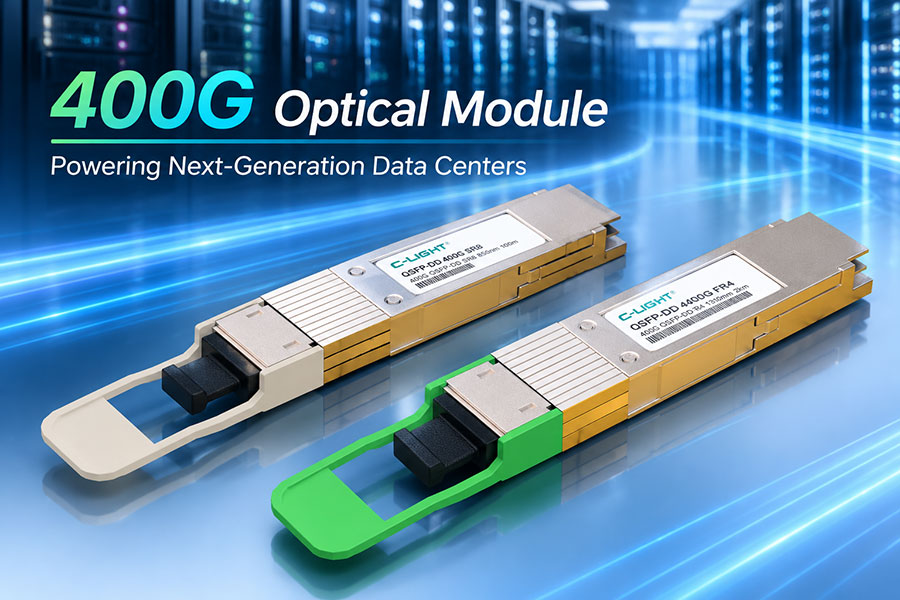
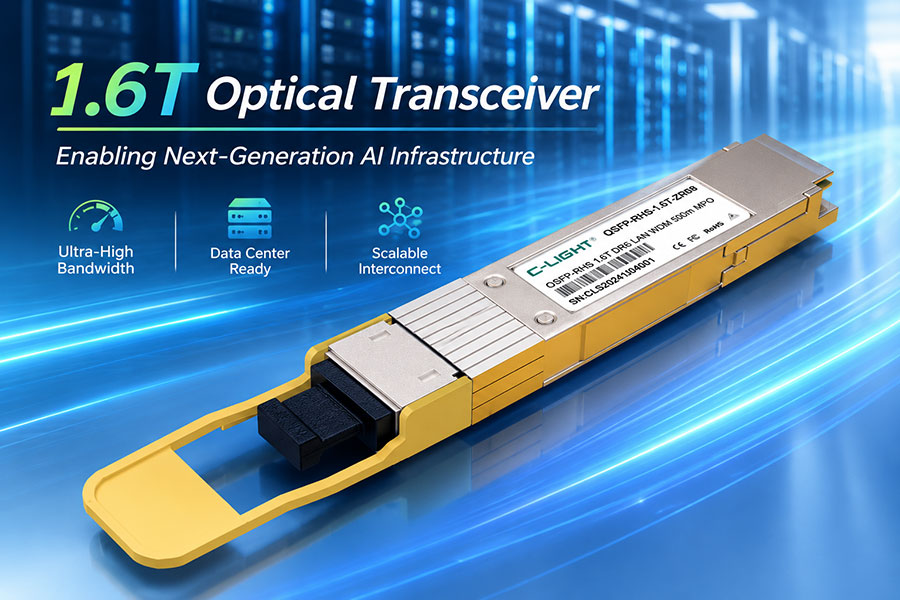
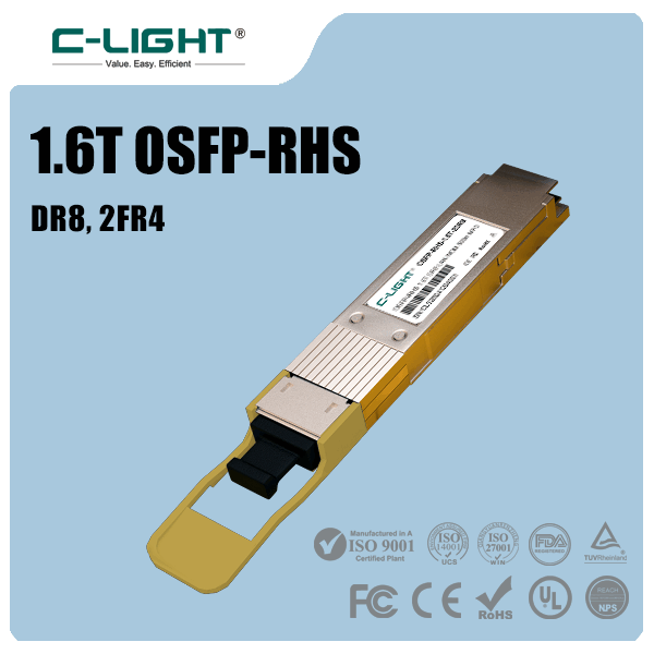
Higher-speed optical transceivers are an important commercial pathway for silicon photonics. As network bandwidth requirements increase, 800G products are being deployed in high-performance environments, while 1.6T designs are advancing to support future generations of AI and cloud infrastructure.
| Market Segment | Primary Demand | Key Considerations |
|---|---|---|
| 400G optical transceivers | Existing data center upgrades and high-speed network connections | Port density, reach, interoperability, and installed network requirements |
| 800G optical transceivers | AI clusters, hyperscale data centers, and high-capacity switches | Thermal design, power consumption, optical performance, and production capacity |
| 1.6T optical transceivers | Next-generation switching and growing AI network bandwidth | Signal integrity, lane speed, packaging, cooling, and system compatibility |
| Integrated optical engines | Higher-density optical links near switches and computing devices | Optical coupling, laser architecture, repairability, and manufacturing yield |
Silicon photonics is not the only technology used in high-speed optical modules. Product selection depends on the required reach, wavelength plan, modulation format, optical architecture, and system design. Market demand for 800G or 1.6T products therefore should not be interpreted as universal adoption of a single photonic platform.
CPO, NPO, and LPO Reshape Optical Integration
The market is expanding beyond conventional pluggable transceivers toward several approaches that bring optical conversion closer to switching and computing silicon. These architectures address different combinations of bandwidth density, power consumption, maintenance requirements, and deployment flexibility.
Co-Packaged Optics
Co-packaged optics (CPO) places optical engines close to or within the same package assembly as a switch ASIC or other high-performance processor. Shorter electrical paths can reduce some high-speed signal transmission challenges and support dense optical connectivity. However, CPO introduces demanding requirements for thermal management, fiber attachment, component replacement, package yield, and system-level testing.
Near-Packaged Optics
Near-packaged optics (NPO) positions optical engines close to the main processing or switching package without necessarily integrating them into the same package. This approach can shorten electrical connections while retaining more modularity than some CPO implementations. NPO is receiving attention as a transition architecture for systems seeking a balance between integration density and serviceability.
Linear Pluggable Optics
Linear pluggable optics (LPO) reduces or removes the conventional DSP function from the optical module signal path in supported system designs. It can lower module power and latency, but places greater demands on host electrical signal quality, link engineering, and system-level interoperability. LPO is an alternative architecture rather than a direct synonym for silicon photonics.
| Architecture | Integration Approach | Potential Advantage | Main Consideration |
|---|---|---|---|
| Pluggable optics | Replaceable module in a host port | Serviceability and established operational workflows | Electrical channel losses and module power at higher speeds |
| LPO | Linear electrical interface with reduced module signal processing | Potential reductions in power and latency | Host signal quality and end-to-end compatibility |
| NPO | Optical engine positioned near the host package | Shorter electrical paths with modularity | Packaging, optical connections, and ecosystem maturity |
| CPO | Optics integrated closely with the main ASIC package | High bandwidth density and potential system-level efficiency | Thermal design, repairability, yield, and fiber management |
These approaches are likely to coexist. Adoption will depend on system requirements, production readiness, cost per bit, reliability targets, and the ability to service deployed equipment.
Manufacturing, Packaging, and Supply Chain Challenges
Market growth depends not only on demand but also on the ability to manufacture and integrate silicon photonics products at scale. Photonic devices combine optical structures with electronic circuits and may require separate laser sources, precision fiber coupling, specialized packaging, and extensive optical and electrical testing.
Optical coupling: Fiber-to-chip alignment and coupling loss affect link performance and assembly yield.
Thermal stability: Temperature variation can shift optical characteristics and affect wavelength control, modulation, and overall performance.
Laser integration: Silicon does not function as an efficient light source by itself in conventional silicon photonics platforms, so external or integrated approaches using other materials may be required.
Testing and yield: Wafer-level screening, packaged-device validation, and high-speed system testing are important for controlling manufacturing costs.
Component availability: Lasers, photodetectors, optical fibers, advanced substrates, and packaging capacity can affect production schedules.
Field maintenance: Integrated optical architectures need practical procedures for fiber handling, fault isolation, and equipment replacement.
As data rates increase, the market advantage will depend on complete system performance rather than the photonic chip alone. Optical engines, electrical interfaces, firmware, fiber management, cooling, and manufacturing processes all contribute to product cost and reliability.
Telecommunications and Emerging Applications
AI data centers are a major growth area, but silicon photonics has potential applications across telecommunications, high-performance computing, sensing, and specialized optical systems. Telecom networks require compact, high-capacity optical components for aggregation, transport, and evolving mobile network infrastructure. Silicon photonics can also support integrated optical functions where size, scalability, and repeatable semiconductor fabrication are important.
Other emerging areas include optical sensing and LiDAR, biomedical instrumentation, and photonic systems for specialized industrial or scientific applications. These markets have different performance and qualification requirements, so their adoption timelines may differ from those of data center optical interconnects.
What Will Shape the Next Stage of Market Growth?
Several factors will influence how quickly silicon photonics moves into wider commercial deployment:
Continued demand for AI computing and high-density data center networking.
Deployment of 800G and 1.6T optical transceivers and the development of faster optical interfaces.
Progress in CPO and NPO integration, including fiber connectivity and serviceability.
Improvements in photonic manufacturing yield, packaging efficiency, and automated testing.
Availability of lasers, photodetectors, optical fibers, and qualified manufacturing capacity.
Demonstrable system-level gains in power, bandwidth density, reliability, and cost per transmitted bit.
Market forecasts should be interpreted alongside deployment evidence. Announced products, engineering samples, pilot systems, and volume shipments represent different stages of commercialization. The most useful indicators are sustained production, validated system performance, customer deployment, and improvements in manufacturing economics.
Conclusion
Silicon photonics is gaining strategic importance as AI data centers and high-performance networks require greater bandwidth density and more efficient optical connectivity. The strongest near-term demand is associated with high-speed optical transceivers, while CPO and NPO create additional opportunities to integrate optics closer to computing and switching silicon.
Long-term market expansion will depend on more than increasing data rates. Manufacturing yield, thermal stability, laser supply, optical coupling, testing, serviceability, and total system cost will determine how broadly silicon photonics can be adopted across data center and telecommunications infrastructure.
Review transceiver options, transmission requirements, and host-system compatibility before selecting an optical interconnect solution.
Contact C-LIGHT >

 >
 >
 >
 >
 >
 >
 >