TEL:+86 132 6656 7067





Signal integrity (SI) testing is essential for validating 800G optical modules used in high-density data center and AI networking systems. At these data rates, electrical channel loss, impedance discontinuities, crosstalk, jitter and transmitter or receiver limitations can reduce operating margin and increase transmission errors. A structured SI test plan evaluates the electrical host interface, the module's internal signal path and the optical link under defined operating conditions.
Successful validation requires more than confirming that an 800G module is detected by a switch or that its optical output power is within specification. Engineers must evaluate high-speed electrical signaling, modulation quality, timing behavior and end-to-end error performance using test methods appropriate to the specific module and interface.
1. What Is Signal Integrity Testing for 800G Optical Modules?
Signal integrity testing assesses whether high-speed signals preserve the electrical and timing characteristics needed for reliable data transmission. For pluggable optical modules, the electrical interface between the host and module is a major part of the SI evaluation. The optical transmitter and receiver introduce additional performance requirements that must be tested separately and, where appropriate, as part of an end-to-end link.
800G modules commonly use multiple high-speed lanes and PAM4 signaling, but lane counts, signaling rates and electrical architectures vary by implementation. The relevant specification determines the required measurements and acceptance limits.
2. Main SI Challenges in 800G Modules
High-Speed Electrical Channel Loss
Electrical signals experience frequency-dependent attenuation as they travel through PCB traces, vias, connectors and module contacts. At high symbol rates, channel loss can reduce signal amplitude and distort transitions, making the receiver's equalization capability increasingly important.
Impedance Discontinuities and Reflections
Changes in impedance along the signal path can reflect part of the incident electrical waveform. These reflections may create ringing, deterministic jitter and inter-symbol interference. The host PCB, connector transition and module input or output structure must be evaluated as a connected high-speed channel.
Crosstalk Between Lanes
Adjacent high-speed lanes can couple through electromagnetic fields. Crosstalk introduces unwanted energy into the victim channel and can reduce eye opening or increase error probability. Dense routing and connector structures make lane isolation an important design consideration.
Jitter and Timing Margin
Jitter shifts signal transitions away from their expected timing positions. Excessive jitter reduces the time available for reliable symbol decisions and can cause the receiver to sample during transitions. Clock generation, channel response, noise and data-dependent effects can all contribute.
PAM4 Signal-Level Margin
PAM4 encodes information using four signal levels, creating three vertical eye openings. The separation between adjacent levels is smaller than in a comparable two-level signaling scheme with the same total amplitude range. Noise, distortion and crosstalk can therefore consume a significant portion of the available decision margin.
3. SI Test Parameters for 800G Optical Modules
| Parameter | Purpose | Typical Measurement Approach |
|---|---|---|
| Insertion loss | Quantifies signal attenuation through an electrical channel | Vector network analyzer or suitable channel characterization setup |
| Return loss | Evaluates reflected energy caused by impedance mismatch | Vector network analyzer or calibrated network measurement |
| Near-end and far-end crosstalk | Characterizes unwanted coupling between electrical lanes | Multiport network analysis and interface-specific channel measurements |
| Eye diagram | Shows combined timing and amplitude behavior of repeated signal transitions | High-bandwidth oscilloscope with appropriate analysis software |
| Jitter | Characterizes signal timing variation | Oscilloscope-based jitter analysis or prescribed compliance equipment |
| Transmitter waveform quality | Evaluates optical signal quality at the transmitter output | Optical reference receiver and standard-specific waveform analysis |
| Receiver sensitivity and tolerance | Evaluates receiver performance under defined input conditions | Controlled optical input, attenuation and BER measurement |
| Bit error rate | Quantifies transmission errors over a defined test interval | Bit error rate tester or compatible traffic test system |
Not every parameter is measured directly at the optical module connector. Electrical channel parameters characterize the high-speed electrical path, while optical waveform and receiver tests characterize the optical interface. A complete validation plan assigns each measurement to its correct reference point.
4. Electrical Channel Characterization
Electrical channel characterization determines whether the host-to-module signal path provides sufficient bandwidth and acceptable reflection and coupling behavior. The evaluation may include the host PCB, connector, module electrical contacts and associated test fixtures.
Insertion Loss
Insertion loss describes the reduction in transmitted signal magnitude through a channel, usually as a function of frequency. Excessive loss can close the eye and increase the burden on transmitter and receiver equalization.
Return Loss
Return loss characterizes the degree of signal reflection at a port or discontinuity. Poor return loss may indicate impedance mismatch, which can contribute to waveform distortion and data-dependent errors.
Crosstalk Measurements
Near-end crosstalk (NEXT) and far-end crosstalk (FEXT) characterize coupling between separate signal paths at defined measurement locations. The required measurements depend on the channel topology and the applicable electrical interface specification.
S-Parameters
Scattering parameters, or S-parameters, describe how high-frequency signals are transmitted and reflected by a network. They are commonly used to characterize insertion loss, return loss and coupling between ports. Accurate results depend on appropriate calibration, fixture de-embedding where required and consistent reference planes.
5. Eye Diagram and PAM4 Analysis
An eye diagram overlays repeated signal transitions to reveal the combined effects of noise, timing variation, channel distortion and other impairments. For PAM4 signals, the waveform produces three eye openings corresponding to the transitions between four signal levels.
Important observations include:
Vertical eye closure: Indicates reduced amplitude margin or increased noise.
Horizontal eye closure: Indicates reduced timing margin or increased jitter.
Uneven signal levels: May indicate transmitter nonlinearity, amplitude imbalance or other waveform impairments.
Pattern-dependent distortion: May reflect inter-symbol interference or channel-response limitations.
For applicable optical PAM4 interfaces, transmitter and dispersion eye closure penalty (TDECQ) is a specified transmitter-quality metric. It is not interchangeable with insertion loss, jitter or BER. Its measurement requires the prescribed optical reference receiver, signal processing and test conditions.
6. Jitter Testing and Timing Margin
Jitter testing evaluates deviations in transition timing and helps identify impairments that may reduce receiver sampling margin. The test objective may be transmitter jitter characterization, host electrical compliance or receiver jitter tolerance.
| Jitter Category | Potential Cause | SI Relevance |
|---|---|---|
| Random jitter | Stochastic circuit and thermal noise | Contributes to statistical timing uncertainty |
| Deterministic jitter | Data-dependent distortion, duty-cycle effects or periodic interference | Can reduce the timing opening of the eye |
| Periodic jitter | Clock coupling, power-supply noise or periodic interference | Can create repeatable timing modulation |
| Data-dependent jitter | Channel bandwidth limitations and inter-symbol interference | Links timing behavior to preceding data patterns |
Measurements should use the pattern, bandwidth, clock recovery settings and analysis method required by the relevant specification. Results obtained using different statistical assumptions or test configurations may not be directly comparable.
7. BER Testing and FEC Performance
Bit error rate testing measures transmission errors over a defined number of compared bits. It provides an end-to-end performance metric that complements electrical and optical waveform measurements.
For 800G links, BER testing should account for the interface's lane architecture, test pattern, modulation format and FEC configuration. Where applicable, pre-FEC BER indicates the error rate before forward error correction, while post-FEC BER reflects errors remaining after correction.
FEC can correct errors within its designed capability, but it does not eliminate the underlying channel impairment. Rising corrected-error counts or an elevated pre-FEC error rate may indicate reduced signal margin, although these symptoms are not unique to SI problems.
8. Recommended SI Testing Workflow
Identify the interface: Confirm the module form factor, host interface, lane configuration, modulation format and applicable compliance specification.
Review the test plan: Separate electrical channel tests from optical transmitter, optical receiver and end-to-end link tests.
Prepare calibrated equipment: Select suitable oscilloscopes, network analyzers, pattern generators, BERT systems and optical measurement equipment.
Verify the fixtures: Confirm calibration, reference planes, connector condition and any required de-embedding.
Characterize the electrical path: Measure the specified insertion loss, return loss and crosstalk parameters.
Evaluate waveform quality: Capture the prescribed electrical or optical waveform and perform the required eye and jitter analysis.
Run receiver and BER tests: Apply the defined input conditions and record error performance, including FEC metrics where relevant.
Document and compare: Record operating conditions, instrument settings, lane identity and results against the correct acceptance limits.
This workflow supports both engineering qualification and troubleshooting. Production test plans may use a reduced set of measurements based on the product requirements and the validated manufacturing process.
9. Common SI Failures and Troubleshooting
Excessive Insertion Loss
Inspect PCB routing, vias, connector transitions, cable assemblies and test fixtures. Confirm that the measured channel includes only the intended reference planes and that fixture effects have been handled correctly.
Poor Return Loss
Investigate impedance discontinuities, connector launches, transitions and grounding or return-path design. Repeat measurements after verifying calibration and fixture condition.
High Crosstalk
Review lane spacing, routing geometry, connector isolation and adjacent signal activity. Compare affected and unaffected lanes using the same measurement setup.
Eye Closure or High Jitter
Check the signal source, channel response, equalization configuration, clock quality and test-system noise floor. Use jitter decomposition and waveform analysis to separate potential contributors.
High BER with Acceptable Optical Power
Average optical power alone does not establish signal integrity. Check transmitter waveform quality, receiver performance, electrical channel characteristics, lane mapping, fiber compatibility and FEC behavior.
Intermittent Link Instability
Correlate errors with temperature, host operating conditions, module diagnostics and lane-level counters. Inspect physical connections and repeat targeted tests under the conditions associated with the fault.
10. SI Validation Across 800G Module Architectures
800G optical modules are available in different form factors and optical implementations. OSFP and QSFP-DD describe module form factors; they do not by themselves specify one universal optical lane arrangement or a single compliance procedure.
| Module Category | Validation Focus | Key Considerations |
|---|---|---|
| 800G OSFP | Host electrical channel, module signal quality and optical interface | Platform design, lane architecture, cooling conditions and interface-specific limits |
| 800G QSFP-DD | Electrical contact path, transmitter and receiver performance | Host implementation, supported module type and applicable compliance requirements |
| Parallel-optical variants | Individual optical lanes and aggregate link performance | Lane mapping, optical path balance and fiber assembly compatibility |
| Wavelength-multiplexed variants | Optical channel quality and wavelength-specific performance | Channel plan, optical filtering and applicable wavelength specifications |
Testing must follow the selected module's actual architecture and datasheet. Form factor alone is not sufficient to infer modulation format, wavelength arrangement, transmitter limits or receiver test requirements.
11. 800G Optical Transceiver Options
When selecting an 800G module, align the optical interface with the host platform, transmission distance, fiber type and network architecture. SI qualification should cover the electrical and optical requirements relevant to that specific configuration.
800G OSFP Optical Transceivers
For supported high-bandwidth network platforms. Confirm the required optical interface, host compatibility and lane-specific validation requirements.
View 800G OSFP Products800G QSFP-DD Optical Transceivers
For compatible 800G network equipment requiring form-factor-specific electrical and optical performance validation.
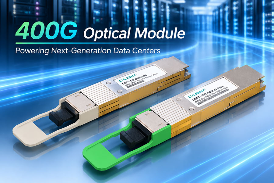
View 800G QSFP-DD Products400G QSFP-DD Optical Transceivers
For 400G links and related network architectures where channel characterization and interface compliance remain essential.
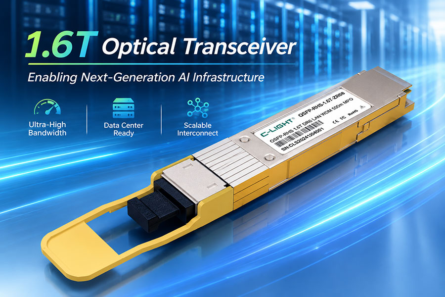
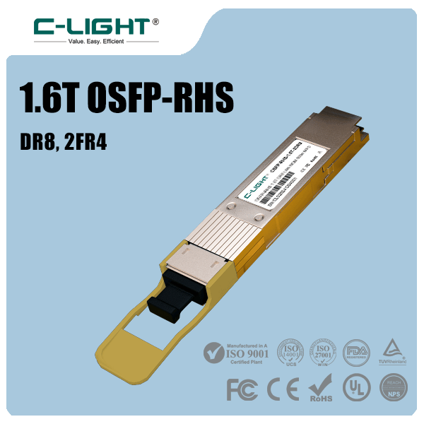
View 400G QSFP-DD Products1.6T OSFP-RHS Optical Transceivers
For next-generation high-density networking platforms. Verify the exact host and optical interface requirements before defining the SI test plan.
View 1.6T OSFP-RHS Products12. Frequently Asked Questions
It evaluates relevant high-speed signal characteristics, which may include electrical channel loss, reflections, crosstalk, jitter, eye quality and BER. The exact test set depends on the module architecture and applicable specification.
No. Optical power testing measures optical power at a defined point. SI testing covers a broader set of electrical and optical signal-quality characteristics, including timing, waveform distortion and error performance.
S-parameters characterize transmission, reflection and coupling in high-frequency channels. They help engineers assess whether the host-to-module electrical path meets the channel requirements for reliable signaling.
Yes. The deployed system may introduce different host conditions, fiber loss, optical compatibility issues, thermal conditions or interoperability problems. Qualification should reflect the intended platform and link configuration whenever possible.
No universal rule can be inferred from the aggregate data rate alone. The signaling format and measurement requirements must be determined from the specific interface specification and module implementation.
No. FEC corrects certain transmission errors within its capability. Poor channel quality, excessive jitter or other impairments can still reduce margin and cause errors beyond the correction limit.
13. Conclusion
SI testing for 800G optical modules requires a coordinated evaluation of high-speed electrical channels, waveform quality, timing behavior and end-to-end transmission performance. Insertion loss, return loss, crosstalk, jitter and BER each reveal different aspects of link health and should be interpreted at the appropriate measurement point.
A reliable validation program uses calibrated equipment, controlled fixtures, lane-aware measurements and acceptance criteria tied to the exact interface specification. Combining electrical characterization with optical testing and BER analysis helps identify design limitations, improve interoperability and maintain operating margin in high-speed data center networks.
Planning an 800G or next-generation optical network?
Review optical module options based on data rate, reach, fiber type and host interface requirements.
Contact C-LIGHT >

 >
 >
 >
 >
 >
 >
 >