TEL:+86 132 6656 7067





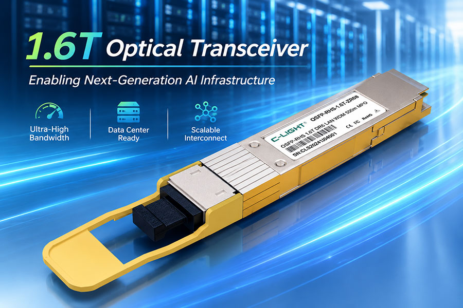
800G and 1.6T optical transceivers concentrate increasingly complex electrical and photonic functions into compact pluggable modules. Higher-speed SerDes interfaces, digital signal processing (DSP), optical drivers, modulators and receiver electronics all contribute to the power budget. In AI data centers, where hundreds of high-speed optical ports may operate simultaneously, the resulting heat load affects switch design, port population, cooling capacity and total operating cost.
The transition from 800G to 1.6T does not simply double module power in every implementation. Aggregate bandwidth, lane rate, modulation, transmission reach, signal-processing architecture and form factor all influence the final result. The engineering objective is to increase throughput while reducing energy per transmitted bit and keeping the complete link within its electrical and thermal operating limits.
1. 800G vs. 1.6T: Power Consumption and Energy per Bit
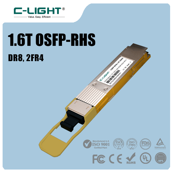
Power figures must be associated with a specific module design rather than treated as universal limits for an entire data-rate class. As a broad planning reference, many conventional 800G datacom pluggables fall around 14–17 W, while many fully retimed 1.6T datacom designs target or operate in roughly the 20–30 W range. Actual values vary by product, reach, optical architecture, temperature and whether the published figure represents typical or maximum power.
| Parameter | 800G Optical Transceiver | 1.6T Optical Transceiver |
|---|---|---|
| Aggregate data rate | 800 Gb/s | 1.6 Tb/s |
| Illustrative module power | 14–17 W for many conventional datacom designs | Approximately 20–30 W for many fully retimed datacom designs |
| Common high-speed lane architecture | Eight 100G-class lanes in many implementations | Eight 200G-class lanes in many implementations |
| Electrical design pressure | High-speed signal integrity, equalization and thermal control | Higher lane rates, tighter channel-loss budgets and greater power-delivery density |
| Primary efficiency objective | Reduce power per bit while sustaining link margin | Increase aggregate throughput without proportional growth in power and heat |
These ranges are indicative, not specifications for every module. Short-reach direct-detect products, low-power architectures and coherent transceivers can have substantially different power profiles. Product datasheets and host-platform requirements should take precedence over generic class averages.
Energy per bit provides a useful way to normalize module power against throughput. It does not, by itself, describe total system efficiency, because the host ASIC, optical line system and cooling infrastructure also consume power.
For illustration, an 800G module consuming 16 W delivers approximately 20 pJ/bit. A 1.6T module consuming 25 W delivers approximately 15.6 pJ/bit. In this example, the 1.6T module consumes more absolute power but delivers lower module-level energy per bit. These calculations are illustrative and should not be interpreted as measurements of specific products.
2. Where the Power Goes Inside an Optical Transceiver
Transceiver power is distributed across several functional blocks. Their relative contribution changes with data rate, reach, DSP architecture and optical implementation. At 800G and 1.6T, the host-side electrical interface and high-speed signal-processing chain can be as important as the photonic devices themselves.
| Subsystem | Power-Consuming Functions | Engineering Factors |
|---|---|---|
| DSP and high-speed electrical interface | Retiming, equalization, signal recovery and digital processing | Lane rate, process technology, channel loss, algorithm complexity and implementation efficiency |
| Transmit driver and modulator | Electrical drive for EML, silicon photonics modulators or other optical transmitters | Required drive swing, modulation efficiency, bandwidth and electrical loading |
| Laser source | Generation of the optical carrier | Laser efficiency, output power, coupling loss, wavelength and temperature |
| Receiver and TIA | Photodetection and amplification of weak electrical signals | Receiver sensitivity, bandwidth, noise performance and optical power budget |
| ADC and DAC functions | Conversion between analog waveforms and digital processing domains where implemented | Sampling rate, resolution, analog bandwidth and architecture |
| Control and power management | Module monitoring, regulation and management interfaces | Voltage conversion efficiency, operating conditions and component integration |
DSP is often a major contributor in fully retimed high-speed modules, but assigning it a fixed percentage across all 800G or 1.6T designs would be misleading. Host SerDes, converters, optical drivers and other circuitry can also consume substantial power. A meaningful power breakdown requires measurements or specifications for the actual implementation.
3. Why 200G-Class Lanes Make 1.6T More Demanding
Many 1.6T datacom architectures use eight 200G-class lanes, compared with eight 100G-class lanes in common 800G designs. Increasing the per-lane data rate reduces the number of parallel lanes needed for a given aggregate bandwidth, but it places tighter constraints on the electrical channel and optical components.
At higher signaling rates, insertion loss, reflections, crosstalk, jitter and frequency-dependent channel behavior become increasingly difficult to manage. Equalization can compensate for part of the channel response, but the required processing and analog circuitry have power costs. Transmitter linearity, receiver noise and clock recovery must also maintain sufficient margin for the target bit-error performance.
The host-to-module electrical connection is particularly important. PCB traces, connectors, package routing and module contacts all contribute to channel loss. At 1.6T, a design that is adequate for an earlier lane rate may require changes to PCB materials, routing topology, connector design or the position of the optical engine.
Higher data rates therefore create a coupled optimization problem: reducing power cannot come at the expense of electrical signal quality, while improving signal quality through more aggressive processing can increase power and heat. The best result depends on co-design across the switch ASIC, electrical interface, optical engine and module packaging.
4. DSP-Based Optics, LPO and LRO
Fully retimed pluggable optics use a module-side DSP to condition or recover high-speed signals. This supports a more controlled electrical interface between host and module and can improve tolerance to channel impairments. The trade-off is the power consumed by the DSP and its associated high-speed analog circuitry.
Linear pluggable optics (LPO) reduce module-side processing by relying more heavily on the host ASIC's electrical interface and signal-conditioning capability. Linear receive optics (LRO) use a hybrid approach in which selected functions remain retimed while others use a more direct electrical path. Exact implementations vary by vendor and product.
| Architecture | Power Strategy | Primary Trade-Off |
|---|---|---|
| Fully retimed pluggable optics | Uses module-side DSP for signal conditioning and recovery | Higher module power, with a more actively conditioned host-module interface |
| LPO | Removes module DSP functions and relies more on host SerDes and linear analog circuitry | Lower potential module power, but tighter channel requirements and greater dependence on host implementation |
| LRO | Retains selected retiming functions while simplifying other signal paths | Intermediate architecture with power savings dependent on the specific implementation |
| NPO and CPO | Move optical engines closer to the host ASIC to reduce high-speed electrical path length | Potential system-level power benefits, balanced against packaging, serviceability and thermal constraints |
Removing a DSP does not eliminate signal-processing requirements; it changes where the functions are performed and how the link is engineered. LPO can reduce module power, but it places greater demands on host electrical performance, channel design and interoperability. The system must still satisfy the required optical and electrical performance targets.
For a fair comparison, engineers should evaluate the complete host-to-host link, including the switch ASIC, module, cable or fiber plant, and any additional processing required to maintain the target error performance.
5. Silicon Photonics and Optical-Engine Efficiency
Silicon photonics integrates optical functions such as waveguides, modulators and photodetectors into a photonic integrated circuit. This can improve integration density and support compact optical engines, particularly as lane counts and aggregate bandwidth increase.
However, silicon photonics is not automatically lower power than every alternative. Total consumption depends on the laser source, modulator efficiency, driver requirements, receiver circuitry, coupling losses and the DSP architecture. An efficient photonic integrated circuit may still be paired with a power-hungry electrical interface or signal-processing chain.
One important design objective is to reduce the electrical distance between the switch ASIC and optical conversion point. Shorter high-speed electrical paths can reduce channel loss and may lower the equalization burden. This is a key reason near-packaged optics (NPO) and co-packaged optics (CPO) are being evaluated for high-bandwidth switching systems.
These architectures introduce additional integration challenges. Optical alignment, package yield, thermal isolation, fiber attachment and field replacement procedures become more complex when optical engines move closer to the ASIC. Their system-level benefits must be assessed against the practical requirements of manufacturing, reliability and maintenance.
6. Thermal Management and Switch-Level Power Budgets
Every watt consumed by a transceiver becomes heat that the system must remove. As modules operate at higher power within increasingly dense switch front panels, thermal design affects the number of ports that can be populated, achievable ambient temperature, fan requirements and long-term operating stability.
For a switch populated with many high-speed optical modules, the aggregate optical power can reach hundreds of watts or more. The switch ASIC, memory, voltage regulators and fans add to the total thermal load. Consequently, a module that meets its individual power specification may still create a platform-level challenge when deployed at full port density.
For example, 64 modules operating at 16 W each consume 1,024 W in aggregate. At 25 W per module, the same number of modules would consume 1,600 W. These figures describe the optical modules alone, excluding the switch ASIC, fans, power conversion losses and other components.
Thermal qualification should consider more than average power. Engineers need to verify maximum operating power, airflow impedance, inlet temperature, heatsink or cold-plate performance, module temperature limits and the host platform's supported thermal configuration. Liquid cooling may be appropriate for some high-density systems, but it is not automatically required for every 1.6T deployment.
7. Measuring Power Efficiency in Real Deployments
Datasheet power is useful for component selection, but it does not fully characterize energy efficiency under production conditions. The actual operating point depends on temperature, traffic configuration, module firmware, optical output requirements, host electrical behavior and platform cooling.
A practical qualification process should distinguish typical operating power from maximum rated power and should record the conditions under which each value was obtained. Measurements should also be consistent across the products being compared.
Module power: Measure or verify electrical consumption under defined operating and temperature conditions.
Energy per bit: Calculate power relative to supported throughput, while keeping the measurement boundary consistent.
Optical performance: Validate transmit power, receiver sensitivity, optical budget and error performance at the required reach.
Host compatibility: Confirm switch support, electrical interface requirements, firmware behavior and module power limits.
Thermal performance: Test under realistic airflow or liquid-cooling conditions with the intended port population.
System-level efficiency: Include host and line-system power where needed to compare complete link architectures.
For high-density AI fabrics, power optimization should be treated as a system design activity rather than a transceiver-only procurement decision. A lower-power module provides limited benefit if it requires additional equipment, reduces link margin or creates interoperability constraints that increase total operating cost.
8. Design Priorities for the Next Generation of Optical Links
Power optimization across 800G and 1.6T is likely to combine several approaches rather than rely on a single component improvement. More efficient DSPs and analog circuits can reduce processing overhead, while better modulator efficiency and optical coupling can lower the electrical power required to produce a usable optical signal.
At the architecture level, LPO and LRO offer ways to reduce selected module-side processing functions. Silicon photonics can support denser optical integration, while NPO and CPO can shorten electrical paths between switching silicon and optical engines. Each approach targets a different part of the power budget and carries its own design constraints.
The most relevant performance target is not simply the lowest module wattage. It is the lowest practical energy per bit that preserves reach, signal integrity, interoperability, reliability and serviceability within the intended network architecture.
9. Conclusion
800G and 1.6T optical transceivers increase network capacity while intensifying electrical, photonic and thermal design requirements. Higher lane rates and more complex signal-processing chains can raise absolute power consumption, but improvements in DSP efficiency, optical-engine design and interconnect architecture can reduce energy per transmitted bit.
Fully retimed optics, LPO, LRO, silicon photonics, NPO and CPO represent different approaches to this problem rather than interchangeable solutions. Selecting the right implementation requires a consistent evaluation of module power, host compatibility, optical performance, thermal limits and total system cost.
10. Frequently Asked Questions
10.1 Why does a 1.6T optical transceiver consume more power than an 800G module?
A 1.6T design handles twice the aggregate bandwidth and commonly uses higher-rate electrical and optical lanes. The resulting demands on SerDes, DSP, drivers, receivers and thermal management can increase absolute power, although the exact increase depends on the architecture.
10.2 Does a lower-power transceiver always provide better energy efficiency?
No. Energy efficiency depends on power relative to throughput and on the measurement boundary. A lower-power module may have different reach, host-interface requirements or operating constraints, so comparisons should use equivalent performance requirements.
10.3 How does LPO reduce optical transceiver power consumption?
LPO removes selected module-side DSP functions and relies more on the host ASIC's high-speed electrical interface. This can reduce module power, but it also places stricter requirements on channel quality, host capability and interoperability.
10.4 Does silicon photonics eliminate the need for a DSP?
No. Silicon photonics integrates optical functions, while DSP performs electrical signal-processing functions. A silicon-photonics transceiver can still use a full DSP, a reduced-processing architecture or another implementation depending on its design.
10.5 What should be checked before deploying 1.6T transceivers?
Verify the exact module specification, host platform support, maximum power, thermal limits, optical interface, link budget, firmware requirements and interoperability. Qualification should cover the intended port population and operating environment.
Evaluating 800G or 1.6T optical connectivity?
Confirm module specifications, host compatibility and optical link requirements for your network design.
Contact C-LIGHT >

 >
 >
 >
 >
 >
 >
 >