TEL:+86 132 6656 7067





High-speed optical receiver design determines how accurately an incoming optical signal can be converted into recoverable electrical data. As Ethernet interfaces advance to 400G, 800G, and 1.6T, receiver sensitivity, bandwidth, noise, linearity, electrical channel quality, and signal processing become increasingly important to reliable optical communication.
1. The Role of Optical Receivers in High-Speed Networks
An optical receiver converts an incoming optical signal into an electrical signal that can be processed by the host system. It is a critical component of an optical transceiver, influencing receiver sensitivity, error performance, supported data rates, and overall link reliability.
In data center networks, the receiver must recover high-speed data despite optical attenuation, electrical noise, signal distortion, and variations in the incoming signal. The design becomes more demanding as lane rates increase because the available time for each symbol becomes shorter and the signal may be more sensitive to channel impairments.
High-speed receiver performance depends on the complete receive chain, not just the photodetector. The photodetector converts light into current, the transimpedance amplifier (TIA) converts that current into a voltage signal, and subsequent circuitry conditions or processes the signal for data recovery.
Depending on the architecture, the receiver may also include equalization, a limiting amplifier, clock and data recovery (CDR), analog-to-digital conversion, and digital signal processing (DSP). The specific implementation depends on whether the transceiver uses direct detection or coherent optical reception.
2. Optical Receiver Architecture and Signal Conversion
A high-speed optical receiver combines optical, analog, and digital functions. These blocks must work together to preserve the information carried by the incoming signal while controlling noise, distortion, power consumption, and latency.
| Receiver Component | Primary Function | Key Design Considerations |
|---|---|---|
| Photodetector | Converts incident optical power into electrical current | Responsivity, bandwidth, capacitance, dark current, and noise |
| Transimpedance amplifier (TIA) | Converts the photodetector current into a voltage signal | Gain, noise, bandwidth, linearity, overload tolerance, and power |
| Analog front end | Conditions the signal for subsequent processing | Frequency response, gain control, linearity, and noise accumulation |
| Equalizer | Compensates for selected frequency-dependent signal distortions | Equalization range, noise enhancement, stability, and implementation complexity |
| CDR | Recovers timing information and retimes the data where implemented | Jitter tolerance, timing recovery, loop behavior, and lock stability |
| ADC and DSP | Digitizes and processes the received signal in architectures that use digital processing | Sampling performance, processing capability, power, latency, and algorithm design |
Not every receiver contains these components as separate blocks. Some functions can be integrated into a single device, while coherent receivers use a different optical front end that includes additional optical mixing and detection functions.
Photodetector performance
The photodetector's responsivity determines how much electrical current is generated for a given optical input power. Its bandwidth and parasitic capacitance influence how quickly the electrical output can follow changes in the optical signal.
Higher responsivity can improve the electrical signal level for a given optical input, but receiver performance also depends on detector noise, capacitance, operating wavelength, and the characteristics of the connected amplifier. A detector selected for a high-speed receiver must meet both the optical and electrical requirements of the design.
Transimpedance amplifier performance
The TIA is one of the most important components in a direct-detection receiver. It converts the small current produced by the photodetector into a usable voltage signal while contributing as little additional noise as practical.
A TIA must balance transimpedance gain, bandwidth, input-referred noise, linearity, and power consumption. Increasing gain may help detect weak signals, but the resulting circuit response and bandwidth must still support the intended signaling rate. The photodetector, TIA, and interconnecting parasitics must therefore be designed as a combined analog front end.
3. Direct-Detection and Coherent Receiver Architectures
The receiver architecture determines how optical information is recovered and which aspects of signal integrity require the greatest attention.
| Characteristic | Direct-Detection Receiver | Coherent Receiver |
|---|---|---|
| Detection principle | Detects optical intensity and converts it into an electrical signal | Combines the received optical field with a local oscillator to recover amplitude and phase information |
| Typical optical front end | Photodetector and TIA | Optical hybrid, photodetector arrays, and associated analog circuitry |
| Signal processing | May use linear or limiting amplification, equalization, CDR, and DSP | Commonly uses high-speed analog-to-digital conversion and DSP for coherent signal recovery |
| Major design concerns | Receiver sensitivity, intensity noise, bandwidth, and signal distortion | Optical signal-to-noise ratio, phase recovery, polarization handling, ADC performance, and DSP |
| Typical applications | Many short-, medium-, and extended-reach Ethernet optical interfaces | Coherent DCI, metro transport, and long-distance optical transmission |
Direct detection is widely used in data center optical links because it can provide an effective balance of performance, implementation complexity, and power consumption for supported reaches. Coherent reception is valuable where recovering more information about the optical field enables higher spectral efficiency or longer-distance transmission.
These architectures have different performance metrics and should not be evaluated using identical assumptions. Direct-detection receiver sensitivity is commonly considered alongside received optical power and bit error rate, while coherent-system design also places significant emphasis on optical signal-to-noise ratio, modulation format, phase recovery, and the optical line system.
4. Bandwidth, Rise Time, and High-Speed Signal Recovery
The receiver bandwidth must be sufficient to preserve the signal transitions and frequency content required by the selected modulation format. Inadequate bandwidth can attenuate high-frequency components, broaden signal transitions, and increase intersymbol interference (ISI).
Bandwidth is not the only determinant of performance. Excessive noise, poor frequency-response flatness, impedance discontinuities, and improper equalization can degrade the recovered signal even when the nominal bandwidth appears sufficient.
In a simplified single-pole system, the relationship between bandwidth and rise time is often approximated by:
This approximation can be useful for understanding first-order system behavior, but it should not be applied as a complete receiver design rule. Actual high-speed receivers have frequency-dependent responses, multiple poles and zeros, and signal-processing stages whose combined behavior affects eye opening and error performance.
Bandwidth versus noise
Increasing receiver bandwidth allows more high-frequency signal content to pass, but it can also admit additional noise. Designers therefore need enough bandwidth to recover the target signal without unnecessarily increasing noise or power consumption.
The optimal response depends on the symbol rate, modulation format, photodetector characteristics, TIA design, channel response, and equalization strategy. Receiver bandwidth should be selected as part of the complete signal chain rather than as an isolated specification.
5. PAM4 Signaling and Receiver Linearity
PAM4 is widely used in high-speed optical and electrical interfaces because it carries two bits per symbol using four signal amplitude levels. This increases the information carried per symbol compared with binary NRZ signaling, which uses two levels.
However, the spacing between adjacent PAM4 levels is smaller for a comparable overall signal range. Noise, distortion, and amplitude variation can therefore make it more difficult to distinguish neighboring levels at the receiver.
Why linearity matters
In a PAM4 receiver, the relationship between the input signal and the electrical output must remain sufficiently linear across the relevant signal range. Compression, gain variation, clipping, or uneven response can change the relative spacing of the signal levels and degrade the receiver's decision margins.
Photodetector behavior, TIA linearity, gain control, and subsequent analog circuitry all influence the recovered signal. Equalization and DSP may compensate for selected distortions, but they cannot remove every impairment or recover information that has been lost through severe clipping or inadequate signal-to-noise ratio.
Signal-level separation and noise margin
The receiver must distinguish the four PAM4 levels accurately over the expected range of optical input powers and operating conditions. Signal-to-noise ratio, frequency response, jitter, and receiver linearity determine how much margin remains between the decision thresholds.
High-speed receiver validation should therefore examine signal quality and error performance rather than relying solely on the measured optical power or the existence of a stable link.
6. Signal Integrity in the Receiver Electrical Path
After optical-to-electrical conversion, the signal passes through sensitive analog circuitry and high-speed interconnects. Poor electrical channel design can degrade the signal before it reaches the data-recovery circuitry, reducing the benefits of an otherwise capable optical front end.
| Signal-Integrity Factor | Potential Effect | Design Approach |
|---|---|---|
| Insertion loss | Attenuates higher-frequency signal components and reduces available signal amplitude | Optimize channel length, interconnect structure, and materials for the target frequency range |
| Return loss | Reflections caused by impedance discontinuities distort the electrical signal | Maintain controlled impedance and minimize abrupt transitions in the signal path |
| Crosstalk | Coupling from adjacent signals introduces unwanted disturbance | Review spacing, routing topology, shielding, and return-current paths |
| Parasitic capacitance | Reduces bandwidth and can affect stability at the photodetector or amplifier input | Minimize sensitive interconnect length and optimize packaging and component layout |
| Power-supply noise | Can modulate analog gain, increase noise, or affect timing and control circuitry | Use appropriate power distribution, decoupling, and isolation between noisy and sensitive blocks |
| Grounding and return paths | Can create unwanted coupling, common-mode disturbance, and reference instability | Maintain clear return-current paths and a suitable grounding strategy |
| Connector and package transitions | Create discontinuities and additional loss in high-speed interconnects | Validate the complete package, board, connector, and host-channel response |
At high signaling rates, seemingly small parasitic effects can meaningfully influence receiver performance. Photodetector-to-TIA connections are especially sensitive because the input signal may be weak, and the input capacitance directly affects the analog front end's frequency response.
Signal-integrity evaluation should cover the entire electrical path, including the receiver package, PCB traces, vias, connectors, host interface, and any intermediate conditioning circuits. A component-level simulation or measurement is valuable, but system-level verification is necessary to confirm that the complete channel meets its requirements.
7. Noise Sources and Receiver Sensitivity
Receiver sensitivity describes the minimum optical input power at which a receiver meets a specified performance target under defined test conditions. It depends on the receiver's noise characteristics, optical signal quality, modulation format, and the bit error rate or other criterion used to define acceptable performance.
In a direct-detection receiver, important noise contributions may include thermal noise from electronic circuitry and shot noise associated with photodetection. The incoming optical signal and transmitter characteristics can introduce additional impairments, while electrical interference and imperfect signal conditioning can degrade the overall result.
Thermal and electronic noise
Electronic noise from the TIA and subsequent analog stages can obscure small received signals. Reducing input-referred noise helps improve sensitivity, but noise optimization must be balanced against bandwidth, gain, stability, power, and linearity requirements.
Shot noise
Photodetection involves discrete charge generation, which produces shot noise associated with the photocurrent and relevant background or dark-current contributions. Its impact depends on the optical input and detector operating conditions.
Signal distortion and intersymbol interference
ISI occurs when a signal transition or pulse affects the interpretation of neighboring symbols. It can result from limited bandwidth, frequency-response distortion, dispersion in the optical path, or reflections and losses in the electrical channel.
Receiver equalization can reduce some forms of ISI, but it may also enhance noise. The design should optimize the overall signal-to-noise ratio and error performance instead of maximizing equalization strength in isolation.
Receiver sensitivity and overload
A receiver must operate across the optical input range specified for its intended application. Sensitivity defines a lower operating boundary under the specified performance conditions, while overload or maximum input power defines an upper boundary.
Testing should verify both limits where required. Sufficient optical power does not guarantee good signal quality, and excessively high received power can also impair operation if it exceeds the receiver's supported range.
8. Equalization, CDR, and Digital Signal Processing
Equalization and signal processing compensate for selected impairments introduced by the optical receiver, electrical channel, and transmission system. Their role becomes increasingly important in high-speed interfaces where the receiver has limited margin for distortion and timing errors.
Continuous-time linear equalization
A continuous-time linear equalizer (CTLE) shapes the analog frequency response to compensate for channel loss. It can restore some high-frequency content before later processing, improving signal transitions and eye opening when applied appropriately.
Equalization settings must be selected carefully because boosting high-frequency content can also amplify noise. The best setting depends on the received signal quality and the frequency response of the full channel.
Decision feedback equalization
Decision feedback equalization (DFE), where implemented, uses previous symbol decisions to compensate for selected post-cursor intersymbol interference. It can improve signal recovery in channels with significant memory, but its performance depends on decision accuracy and implementation details.
Clock and data recovery
CDR circuitry recovers timing information from the received data and establishes sampling points for data recovery. Jitter, signal distortion, and insufficient transition information can affect timing recovery or reduce the margin available at the sampling instant.
Digital signal processing
DSP can implement equalization, symbol detection, clock recovery, and other signal-processing functions, depending on the receiver architecture. Coherent receivers use more extensive digital processing to recover amplitude and phase information, while direct-detection modules may use different processing paths according to the optical interface.
Processing capability is not unlimited. The receiver must balance equalization performance, error correction, latency, implementation complexity, and power consumption within the module's system constraints.
9. Receiver Design for 400G, 800G, and 1.6T Optical Modules
High-speed optical modules require a coordinated design across the photodetector, analog front end, host electrical interface, and signal-processing path. As per-lane signaling rates increase, the channel must preserve the required signal characteristics over shorter symbol intervals and tighter design margins.
| Optical Interface Class | Receiver Design Priorities | System-Level Considerations |
|---|---|---|
| 100G | Receiver sensitivity, bandwidth, noise, and optical interface compatibility | Validate the exact physical layer, host signaling, reach, and required FEC behavior |
| 400G | Multi-lane consistency, PAM4 signal quality where applicable, equalization, and receiver performance | Check lane mapping, optical architecture, error counters, and host-channel characteristics |
| 800G | High-speed analog bandwidth, low-noise front end, linearity, lane diagnostics, and timing recovery | Confirm electrical interface support, module power, cooling, and specified optical behavior |
| 1.6T | 200G-class lane implementations where applicable, advanced analog design, signal processing, and tighter channel margins | Validate the actual lane architecture, module implementation, host platform, and complete link performance |
These categories describe broad engineering priorities, not one universal receiver architecture per data rate. Different interfaces at the same aggregate bandwidth may use different modulation formats, lane arrangements, optical technologies, and signal-processing implementations.
For example, some data center transceivers use direct-detection PAM4 receivers, while coherent 800G modules use a different receiver structure optimized for coherent signal recovery. The design methods and acceptance criteria must match the actual interface.
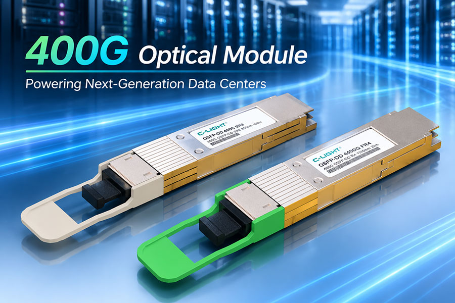
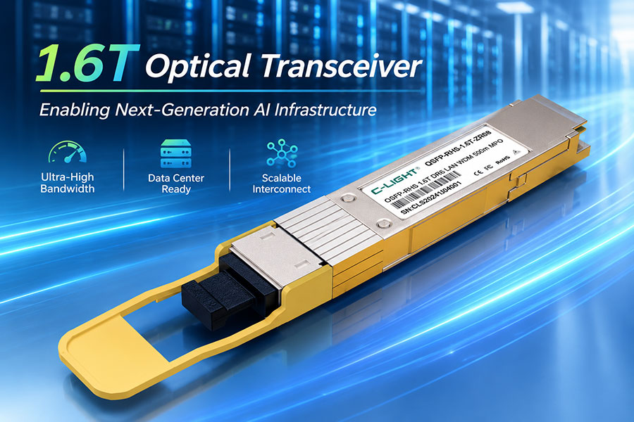
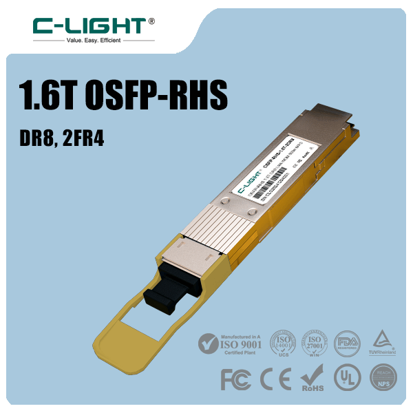
For platform integration, review the relevant 400G QSFP-DD, 800G OSFP, and 1.6T OSFP-RHS configurations. Confirm the selected module's optical interface, receiver specifications, host compatibility, and required operating conditions.
10. Testing and Validating Receiver Signal Integrity
Receiver qualification should combine optical measurements, electrical signal analysis, error-performance testing, and environmental verification. No single measurement can establish the performance of the entire receive chain.
| Test Method | What It Evaluates | Purpose |
|---|---|---|
| Optical power measurement | Optical power at a defined point in the test setup | Verifies input conditions and supports receiver power-budget analysis |
| Receiver sensitivity test | Performance at low optical input power | Determines whether the receiver meets its specified error-performance criterion |
| Eye diagram analysis | Amplitude separation, timing margin, noise, and signal distortion | Provides a visual and quantitative view of signal quality at the applicable measurement point |
| Jitter measurement | Timing variation in the received signal or recovered clock | Checks timing margin and relevant compliance limits |
| BER testing | Bit errors under defined test conditions | Evaluates end-to-end data recovery performance |
| FEC analysis | Corrected and uncorrectable errors where exposed | Helps evaluate signal quality and error-correction behavior |
| Frequency-response measurement | Bandwidth, peaking, and channel loss over frequency | Identifies limitations in the analog front end or electrical channel |
| Thermal and stability testing | Performance across supported operating conditions and time | Verifies that receiver behavior remains within specification under representative conditions |
Tests should use the optical input conditions, pattern, operating mode, and measurement points defined for the applicable interface. Sensitivity results are meaningful only when the target error rate and the influence of transmitter impairments, dispersion, and other test conditions are understood.
Where a receiver is part of a multi-lane interface, testing should evaluate individual lanes when measurement capability permits. Aggregate link performance can conceal a lane-specific problem that only becomes apparent through lane-level error or signal-quality data.
11. Common Receiver Signal-Integrity Problems
| Observed Symptom | Possible Cause | Recommended Investigation |
|---|---|---|
| Poor receiver sensitivity | Excessive electronic noise, insufficient bandwidth, detector limitations, or an impaired optical signal | Verify optical input conditions, measure error performance, and review the photodetector and analog front end |
| Reduced eye opening | Channel loss, crosstalk, jitter, ISI, or receiver nonlinearity | Examine the electrical channel response, signal amplitude, timing, and equalization settings |
| High error rate despite acceptable Rx power | Signal distortion, noise, lane problems, or interface configuration issues | Review BER, FEC statistics, electrical signal quality, and lane-level diagnostics where available |
| Unstable clock recovery | Excessive jitter, insufficient transition information, or distorted signal edges | Measure jitter and inspect the signal quality at the applicable clock-recovery input |
| Performance changes at different temperatures | Temperature-dependent analog characteristics, optical output changes, or host thermal limitations | Correlate performance measurements with temperature, module diagnostics, and platform cooling conditions |
| Signal quality worsens after channel changes | Increased insertion loss, return-loss issues, crosstalk, or changed equalization requirements | Re-evaluate channel characteristics and revalidate the electrical interface configuration |
| One lane shows more errors than others | Lane-specific optical or electrical impairment, coupling issue, or component variation | Compare per-lane signal measurements, optical power, and relevant error counters |
Receiver troubleshooting should separate optical-path issues from electrical-channel and processing issues. If received power is within specification but error performance is poor, increasing optical power is not necessarily the correct solution. The actual impairment must first be identified.
12. Design Priorities for Reliable High-Speed Receivers
A reliable receiver is the result of coordinated optical, analog, electrical, and digital design. Optimizing one component in isolation can shift the limitation to another part of the signal path.
Optimize the photodetector and TIA together: Consider responsivity, detector capacitance, input-referred noise, gain, bandwidth, and linearity as a combined design problem.
Control electrical parasitics: Minimize unnecessary interconnect length and validate package and PCB effects on the receiver input response.
Maintain signal integrity: Control impedance, insertion loss, return loss, crosstalk, and power-supply noise across the entire electrical path.
Balance equalization and noise: Apply appropriate frequency-response correction without amplifying noise unnecessarily.
Validate PAM4 performance where applicable: Check level separation, receiver linearity, timing margin, and error performance under the specified conditions.
Manage power and temperature: Confirm that the receiver and DSP operate within their electrical and thermal limits during sustained operation.
Use system-level validation: Evaluate the transceiver together with its host platform, optical path, electrical channel, and configuration.
Document test conditions: Record measurement points, patterns, optical input power, firmware, lane configuration, and acceptance criteria so results can be reproduced.
13. Frequently Asked Questions
13.1 What determines the sensitivity of a high-speed optical receiver?
Receiver sensitivity depends on the optical input, photodetector characteristics, TIA noise and bandwidth, subsequent signal conditioning, modulation format, and the specified error-performance criterion. Transmitter quality and other link impairments can also affect measured system sensitivity.
13.2 Why is the TIA important in high-speed optical receivers?
The TIA converts the small current generated by the photodetector into an electrical voltage suitable for downstream processing. Its gain, bandwidth, noise, linearity, and power consumption directly influence the receiver's ability to recover high-speed signals.
13.3 Why does PAM4 require careful receiver design?
PAM4 encodes two bits per symbol using four amplitude levels. The smaller separation between adjacent levels makes the signal more sensitive to noise, distortion, and timing errors than a comparable binary signaling scheme, increasing the importance of receiver linearity and signal-quality control.
13.4 Can equalization solve all signal-integrity problems?
No. Equalization can compensate for selected frequency-dependent impairments, but it may increase noise and cannot fully recover a signal damaged by severe clipping, insufficient signal-to-noise ratio, or other information loss. The channel and receiver should be optimized together.
13.5 Is optical power enough to determine receiver performance?
No. Optical power indicates the amount of received light, but not the complete signal quality. Noise, bandwidth, signal distortion, jitter, modulation, lane performance, and FEC behavior can all affect error performance even when receive power is within its specified range.
13.6 What should be checked when validating an 800G or 1.6T receiver?
Confirm the specific optical interface, lane architecture, optical input range, receiver sensitivity, electrical host interface, signal-integrity requirements, power and thermal limits, diagnostic visibility, and error-correction configuration. Validate the complete link under the intended operating conditions.
14. Summary
High-speed optical receiver design combines photodetection, low-noise amplification, analog signal conditioning, equalization, timing recovery, and digital processing. Receiver sensitivity and signal integrity depend on how these functions interact with the optical signal, electrical channel, and host platform.
As networks progress toward 400G, 800G, and 1.6T interfaces, tighter signal margins and higher per-lane rates increase the importance of bandwidth, linearity, noise control, impedance management, and thermal design. Direct-detection and coherent receivers require different architectures and performance evaluations, but both depend on careful optimization of the complete signal chain.
Reliable receiver validation combines optical power measurements with eye diagrams, jitter analysis, BER testing, lane diagnostics, and thermal verification where applicable. This system-level approach helps identify signal-integrity limitations and supports stable operation in high-capacity data center and optical transport networks.
Developing or deploying high-speed optical networks?
Review the 400G QSFP-DD, 800G OSFP, and 1.6T OSFP-RHS optical transceiver options and confirm their receiver and host-interface requirements.
Contact C-LIGHT >

 >
 >
 >
 >
 >
 >
 >