TEL:+86 132 6656 7067





Data center network design is entering a period of rapid change as AI training, inference and distributed computing increase the amount of data exchanged between processors and switches. Higher port bandwidth, greater connection density and tighter power constraints are putting pressure on conventional electrical interconnects. Silicon photonics offers a scalable way to integrate optical functions into compact devices, supporting the evolution of high-speed transceivers and emerging optical-engine architectures.
The future of silicon photonics will not depend on a single breakthrough. Progress will come from improvements in photonic integration, laser technology, advanced packaging, manufacturing yield and network architecture. Pluggable transceivers will continue to serve many deployments, while linear-drive optics, near-packaged optics and co-packaged optics offer alternative approaches for specific bandwidth and power requirements.
1. Why Silicon Photonics Is Becoming More Important
As network bandwidth increases, the cost of moving data becomes an increasingly important part of data center design. Silicon photonics can address some of the physical limitations of high-speed electrical transmission, but its overall value depends on the link architecture, optical reach, electronic circuitry, packaging and cooling requirements.
2. From 800G to 1.6T and Beyond
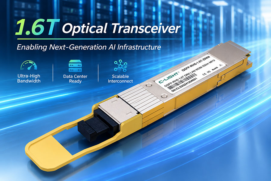
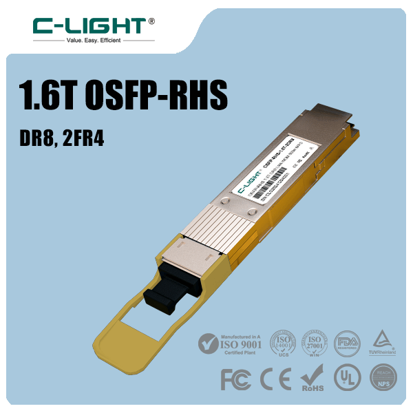
Higher-capacity optical interfaces are a major part of the data center roadmap. The transition from 400G to 800G and 1.6T increases the amount of data carried by each network connection, helping operators build higher-capacity fabrics. Each generation also raises demands on electrical lane rates, optical performance, thermal management and production consistency.
| Technology Generation | Key Engineering Focus | Role in Data Centers |
|---|---|---|
| 400G optical links | Established multi-lane architectures, reach requirements and interoperability. | Continue to support many existing data center and enterprise deployments. |
| 800G optical links | Higher aggregate bandwidth, improved signal integrity and power-aware module design. | Support growing AI clusters and high-capacity switch fabrics. |
| 1.6T optical links | Higher-speed electrical lanes, advanced photonic integration and more demanding thermal budgets. | Provide a path to greater switch-port capacity and dense AI networking. |
| Future higher-capacity links | Further improvements in modulation, photonic integration, packaging and test methods. | Address future bandwidth-density requirements as standards and products mature. |
Many 1.6T designs target 200G-class electrical lanes, but lane counts, modulation formats and optical architectures vary by implementation. Higher aggregate capacity does not automatically mean proportionally higher application throughput, because protocol overhead, congestion and network utilization also affect useful data transfer.
3. Silicon Photonics in AI Data Center Architectures
AI infrastructure includes several communication domains, and each has different requirements for distance, latency, bandwidth and reliability. Silicon photonics can support selected optical interfaces across these domains, but it is not necessary for every connection.
| Network Domain | Connectivity Requirement | Potential Silicon Photonics Role |
|---|---|---|
| Scale-up | High-bandwidth communication between closely coupled accelerators. | Potential role in emerging optical scale-up and optical I/O architectures; many current systems still use electrical or proprietary interconnects. |
| Scale-out | Connections between accelerator servers and Ethernet or InfiniBand switches. | Optical transceivers and optical engines can support high-capacity links across racks and network tiers. |
| Scale-across | Connectivity between clusters, buildings or data center campuses. | Can support selected single-mode and wavelength-multiplexed links, depending on reach and performance requirements. |
| Switch-to-switch | High-radix switching fabrics with increasing aggregate bandwidth. | Supports pluggable optics today and can be used in near-packaged or co-packaged architectures. |
The network protocol and optical technology solve different problems. Ethernet and InfiniBand define communication and transport behavior, while the optical transceiver provides the physical interface. The selected module must match the host port, supported data rate, optical standard, reach and fiber infrastructure.
4. The Evolution from Pluggable Optics to CPO
Pluggable transceivers place the optical engine inside a removable module connected to the host through an electrical interface. This approach offers operational flexibility because modules can generally be replaced independently of the switch ASIC.
As electrical lane rates rise, the board-level channel between the host ASIC and a front-panel module can consume increasing power and signal-integrity margin. Moving optical conversion closer to the ASIC is one strategy for addressing this limitation.
| Architecture | Optical Engine Location | Main Advantage | Primary Trade-Off |
|---|---|---|---|
| Pluggable optics | Inside a removable transceiver module. | Established deployment model and independent module replacement. | Longer electrical path between host ASIC and optical engine. |
| Linear pluggable optics (LPO) | Inside a pluggable module with a simplified signal-processing chain. | Can reduce module power and cost in compatible systems. | Places greater demands on host signal quality and system-level optimization. |
| Near-packaged optics (NPO) | Near the host ASIC, but not necessarily within the same package. | Shortens electrical paths while retaining more separation from the ASIC package. | Requires careful mechanical, electrical, thermal and service integration. |
| Co-packaged optics (CPO) | Within the host ASIC package ecosystem or closely integrated package. | Can substantially shorten high-speed electrical connections. | Raises packaging, fiber access, thermal management and serviceability challenges. |
These architectures are complementary rather than mutually exclusive. Industry analysis published in 2026 describes continued investment in NPO and CPO while expecting pluggable optics to remain a substantial part of the market. Actual adoption will vary by switch platform, customer requirements and the maturity of production ecosystems.
5. Why CPO Is Not the Only Future
CPO attracts attention because it can place optical engines very close to high-bandwidth ASICs, reducing electrical channel length. However, close integration changes how systems are assembled, cooled, tested and repaired. The benefits must be weighed against those operational costs.
NPO can provide an intermediate approach by shortening electrical connections while preserving more physical separation between optical engines and the main ASIC package. LPO can reduce power in selected pluggable designs without requiring the same degree of package integration. Conventional pluggable modules remain useful where field replacement and multi-vendor flexibility are priorities.
Future data centers are therefore likely to use several optical architectures according to the location and function of each link. High-density switch connections, server uplinks and longer-reach data center links do not necessarily require the same technology.
6. Power Efficiency and Thermal Management
Silicon photonics can support power-efficient optical links, but the PIC itself is only one contributor to total energy consumption. Laser sources, modulators, drivers, TIAs, DSPs where used, control circuitry, power delivery and cooling all contribute to the final system budget.
Shorter electrical paths can reduce channel loss and may lower the equalization or retiming effort required in some architectures. Nevertheless, the net benefit must be measured across the complete link, using the same system boundary for each comparison.
Thermal Design Priorities
Keep laser sources and temperature-sensitive photonic devices within their specified operating conditions.
Evaluate local temperature gradients around switching ASICs and optical engines.
Account for wavelength shifts in resonant or wavelength-selective devices.
Optimize heat paths through the package, module housing and system cooling structure.
Validate optical and electrical performance under realistic operating loads.
Thermal design becomes particularly important in dense 800G and 1.6T systems, where higher port counts and aggregate bandwidth can increase heat generation within a limited space.
7. Advances in Photonic Integration and Materials
Silicon photonics benefits from semiconductor fabrication techniques that can produce complex optical circuits at wafer scale. Continued development is focused on integrating more functions, improving device performance and making the resulting optical engines easier to assemble and test.
| Development Area | Technical Direction | Potential Significance |
|---|---|---|
| Photonic integrated circuits | Higher integration density and improved control of optical loss and device variation. | Smaller optical engines and more integrated optical functions. |
| Laser integration | Improved external laser sources and hybrid or heterogeneous integration approaches. | More flexible source placement and potential improvements in package efficiency. |
| High-speed modulators | Higher bandwidth and lower energy per bit within practical optical and electrical constraints. | Support for future high-speed lane architectures. |
| Photonic-electronic integration | Closer integration of PICs with drivers, receivers and host electronics. | Shorter electrical paths and potentially improved bandwidth density. |
| Alternative photonic materials | Use of platforms such as indium phosphide or thin-film lithium niobate where their properties suit the application. | Different trade-offs in modulation, gain, wavelength range, integration and manufacturing. |
Silicon photonics is not expected to replace every other optical material platform. Silicon is attractive for integration and scalable fabrication, while other materials can offer advantages for light generation, high-performance modulation or particular wavelength and reach requirements. Hybrid systems may combine the strengths of multiple materials.
8. Manufacturing Yield and Packaging Will Shape Adoption
As optical engines move toward denser integration, packaging becomes a major determinant of product cost and reliability. The manufacturing process must connect the photonic circuit to fibers, laser sources and high-speed electronics while maintaining optical alignment and electrical performance.
Fiber-to-chip coupling: Alignment errors can increase insertion loss and reduce link margin.
Laser integration: Source placement affects optical routing, thermal isolation and maintenance.
Electrical interconnects: Package parasitics can limit bandwidth and increase signal-conditioning requirements.
Thermal stability: Temperature gradients may affect wavelength, device characteristics and reliability.
Production testing: Wafer-level measurements must be complemented by packaged-device and system-level validation.
Supply-chain capacity: Laser components, photonic dies, fiber arrays and advanced packaging must scale together.
Manufacturing readiness is as important as device performance. A design that works in a laboratory may still need substantial development to achieve consistent coupling, acceptable yield, field reliability and cost-effective high-volume production.
9. Optical I/O and the Next Stage of Integration
Optical I/O aims to bring optical connectivity closer to compute and switching devices, potentially reducing the limitations of conventional electrical connections. Depending on the design, optical interfaces may be integrated near an ASIC, within an advanced package or as part of a larger system-level optical architecture.
These approaches could become more relevant as AI systems require greater bandwidth between processors, memory resources and network fabrics. However, optical I/O faces challenges involving package design, power delivery, thermal behavior, testability, reliability and the interfaces needed to connect optical devices to electronic systems.
Optical I/O should therefore be viewed as an evolving direction rather than a universal replacement for conventional transceivers. Its adoption will depend on whether the benefits justify the additional integration and operational complexity for a given system.
10. What Data Center Operators Should Prepare For
Operators planning new AI infrastructure can prepare for higher optical bandwidth without committing prematurely to a single future architecture. The most useful preparation focuses on flexible fiber infrastructure, consistent link specifications, cooling capacity and deployment procedures.
| Planning Area | Recommended Considerations |
|---|---|
| Bandwidth roadmap | Plan migration across 400G, 800G and 1.6T according to switch generations, workload demand and platform availability. |
| Fiber plant | Validate fiber type, connector formats, cable routes, optical loss and the capacity needed for future port density. |
| Power and cooling | Evaluate module power, switch power, airflow and thermal limits under expected operating loads. |
| Interoperability | Verify transceiver compatibility, host support, optical standards and required firmware behavior. |
| Serviceability | Define replacement, troubleshooting, connector cleaning and spare-parts procedures. |
| Architecture flexibility | Assess pluggable, LPO, NPO and CPO options according to actual link constraints and operational requirements. |
Fiber readiness is particularly important because increasing port speeds do not remove the need for careful physical-layer engineering. Connector cleanliness, cable routing, polarity, labeling and optical loss management remain essential to stable data center operation.
11. Future Outlook: Multiple Architectures Will Coexist
The future of silicon photonics is closely tied to the expansion of AI computing, higher-capacity switching and the need to move data with greater bandwidth density. Its manufacturing advantages and integration capabilities make it an important platform for optical interconnect development, but no single package architecture will fit every application.
In the near term, pluggable transceivers are expected to remain important because of their established deployment model and serviceability. LPO and NPO offer intermediate approaches for selected systems, while CPO targets applications where shorter electrical paths and high integration density can justify more complex packaging. Over time, optical I/O and more advanced photonic-electronic integration may expand the role of optics closer to computing devices.
The pace of adoption will depend on measurable improvements in power, bandwidth density, reliability, manufacturing yield and total cost of ownership. Standards, supply-chain capacity and field-service procedures will be just as important as raw optical performance.
12. Frequently Asked Questions
12.1 Will silicon photonics replace traditional optical transceivers?
Silicon photonics is a technology used inside optical products, including many types of transceivers. It is more accurate to expect continued evolution in transceiver architectures than a simple replacement of transceivers by silicon photonics.
12.2 Will 1.6T become the standard for all data center links?
No. Data centers use different link rates according to switch capacity, reach, cost and workload needs. Higher-speed interfaces will expand where their advantages justify the additional power, thermal and infrastructure requirements.
12.3 Is CPO certain to replace pluggable optics?
No. CPO can improve electrical reach and integration density, but pluggable optics offer operational flexibility and independent replacement. The two approaches are likely to coexist across different systems and deployment stages.
12.4 Does silicon photonics always consume less power?
No. Power depends on the complete optical link, including the laser, drivers, receiver electronics, DSP where used, packaging and cooling. Silicon photonics can enable efficient designs, but the final result must be measured at a consistent system boundary.
12.5 What are the biggest barriers to wider adoption?
Key challenges include packaging yield, optical coupling accuracy, thermal management, high-speed electrical integration, laser supply, testing costs and serviceability. These factors become particularly important as optical engines move closer to high-power ASICs.
13. Conclusion
Silicon photonics is positioned to play an important role in the next generation of data center connectivity. AI workloads and higher-capacity switching are increasing demand for optical links that combine high bandwidth, dense integration and efficient operation.
The path forward will include multiple approaches: established pluggable transceivers, simplified optical modules, near-packaged optics, co-packaged optics and emerging optical I/O. Success will depend on matching each architecture to the required bandwidth, reach, power budget, manufacturing capability and operational model.
Discuss optical transceiver specifications, fiber interfaces and host compatibility requirements with the C-LIGHT team.
Contact C-LIGHT >

 >
 >
 >
 >
 >
 >
 >