TEL:+86 132 6656 7067





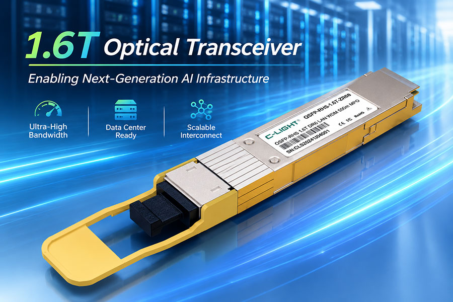
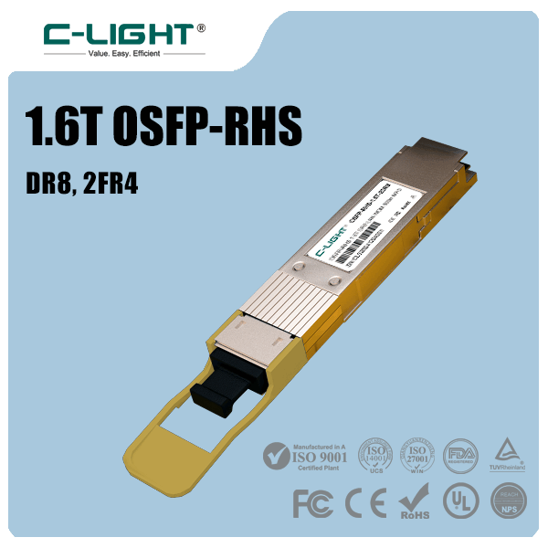
A 1.6T optical transceiver doubles the aggregate bandwidth of an 800G module, commonly by advancing from eight 100G-class lanes to eight 200G-class lanes. This transition places greater demands on electrical channel quality, optical modulation, timing recovery, error performance and thermal design. Digital signal processing (DSP) helps manage these requirements, making it a key component in many next-generation pluggable optical transceivers for AI data centers and high-capacity Ethernet fabrics.
1. Why DSP Matters in 1.6T Optical Transceivers
Higher aggregate bandwidth alone does not define the difficulty of a 1.6T optical link. The more important change is the amount of data carried by each electrical and optical lane. In a common eight-lane design, each lane operates at a 200G-class data rate using PAM4 signaling.
As lane rates increase, electrical channels become more sensitive to frequency-dependent loss, reflections, crosstalk and timing distortion. The optical transmitter and receiver must also maintain sufficient signal quality at higher symbol rates. DSP provides digital signal-conditioning functions that help compensate for these impairments within the limits of the selected architecture.
Depending on the design, a 1.6T DSP may provide:
Transmit equalization and pre-emphasis: Shape the outgoing electrical waveform to compensate for channel response.
Receive equalization: Reduce intersymbol interference and improve symbol detection.
Digital pre-distortion: Compensate for selected transmitter nonlinearity where supported.
Lane mapping: Adapt data between host-side and optical-side lane configurations when required.
FEC-related processing and monitoring: Support the error-control architecture implemented by the device.
Diagnostics: Provide supported signal-quality measurements, test patterns and loopback functions.
Not every 1.6T module implements all these functions in one chip. The DSP may integrate with driver circuitry, use external analog components or provide only selected processing functions, depending on the product design.
2. The 1.6T Architecture and 200G-Class PAM4 Lanes
A common 1.6T client-optics architecture uses eight lanes, each carrying approximately 200G-class data, to reach an aggregate rate of 1.6 Tbps. PAM4 represents two bits per symbol through four amplitude levels, increasing the number of bits transmitted per symbol compared with NRZ signaling at the same symbol rate.
| Architecture | Lane Configuration | DSP Consideration |
|---|---|---|
| 800G reference | 8 × 100G-class lanes | Provides a useful baseline for understanding the increase in lane rate and signal-processing demands. |
| 1.6T eight-lane design | 8 × 200G-class lanes | Requires electrical and optical interfaces designed for the higher lane rate. |
| 1.6T with a 16-lane host interface | 16 × 100G-class electrical lanes mapped to an eight-lane optical interface in supported implementations | May require gearbox or lane-mapping functions between host and optical interfaces. |
| Alternative lane-mapping designs | Depends on the DSP and module implementation | Must be checked against the actual electrical interface, optical engine and product specification. |
The 200G-class lane rate is a nominal interface description, not a guarantee that every implementation uses identical signaling parameters. Actual symbol rates and line bit rates depend on the applicable Ethernet or InfiniBand interface, coding and implementation.
For a typical 200G-class PAM4 lane, the symbol rate is around 106 GBd. That places significant demands on electrical channel bandwidth and the performance of the transmitter, receiver and associated signal-processing circuitry.
3. How DSP Processes High-Speed PAM4 Signals
PAM4 uses four signal levels to represent two bits per symbol. Because the amplitude separation between adjacent levels is relatively small, noise, distortion and timing errors can cause a receiver to misidentify the transmitted symbol. Higher lane rates further tighten the available signal-integrity margin.
In the receive direction, photodetectors convert incoming light into electrical signals. A transimpedance amplifier (TIA) converts the detector current into a usable voltage, after which receiver circuitry and applicable DSP functions help recover the data.
DSP cannot correct every impairment. Excessive optical loss, insufficient receiver power, severe transmitter distortion or operation outside the specified channel limits may still produce unacceptable errors even when the DSP is functioning correctly.
4. Equalization at 200G per Lane
At high symbol rates, electrical-channel losses can significantly distort the transmitted waveform. Frequency-dependent attenuation reduces high-frequency signal components, while impedance discontinuities can create reflections. The resulting intersymbol interference makes it more difficult to distinguish adjacent PAM4 levels.
DSP-based equalization compensates for selected aspects of the channel response. The exact implementation may include feed-forward equalization (FFE), decision-feedback equalization (DFE), transmit pre-emphasis or other algorithms suited to the interface.
| DSP Function | Primary Purpose | Design Relevance at 1.6T |
|---|---|---|
| Transmit FFE | Shapes the outgoing waveform | Helps compensate for expected electrical-channel loss. |
| Receive FFE | Adjusts signal response before symbol decisions | Reduces selected forms of channel-induced distortion. |
| DFE | Uses previous symbol decisions to mitigate postcursor interference | Can improve detection when supported by the receiver architecture. |
| Digital pre-distortion | Compensates for selected nonlinear behavior in the transmit path | Can improve transmitter signal quality when matched to the device and optical components. |
| Adaptive processing | Adjusts processing parameters within supported operating limits | Helps accommodate variation in channel response and operating conditions. |
The DSP does not operate independently of the host channel. Package traces, connectors, board materials, the module electrical interface and the ASIC SerDes all contribute to the complete channel response. The design must allocate signal-integrity margin across these components rather than relying on the module DSP to compensate for an arbitrarily poor channel.
5. Lane Mapping, Gearbox and Retiming
Lane mapping becomes important when the host electrical interface does not match the optical lane configuration. For example, a supported design may accept sixteen 100G-class host lanes and map them to eight 200G-class optical lanes. A different design may use eight 200G-class lanes on both sides.
A gearbox performs data-rate or lane-count conversion. Retiming restores a timing reference and regenerates signals through a defined transmit or receive path. These functions are related but not identical, and their presence depends on the selected DSP architecture.
When host and optical interfaces already use compatible eight-lane 200G-class configurations, the same lane-count conversion may not be needed. Product selection should therefore be based on the actual interface specification, rather than assuming that every 1.6T DSP includes an identical gearbox.
6. FEC and Error Performance
Forward error correction (FEC) adds coding redundancy that allows the receiver to detect and correct a defined range of transmission errors. At 200G-class lane rates, FEC architecture is an important part of maintaining the required link error performance.
DSP and FEC address different problems. Equalization and symbol detection improve the quality of the recovered signal, while FEC processes coded data to correct supported errors. Depending on the implementation, FEC may be located in the host Ethernet PCS, the module DSP, a coherent line-processing device or a combination of system components.
| Parameter | What It Indicates | How It Is Used |
|---|---|---|
| Pre-FEC BER | Error rate before the relevant FEC decoder | Indicates the error burden presented to the correction process. |
| Post-FEC BER | Residual error rate after FEC processing | Helps assess whether the link meets the required error performance. |
| Corrected-error statistics | Errors handled by the FEC decoder, when exposed | Can reveal changes in link margin before an outage occurs. |
| Signal-quality metrics | Measurements such as SNR or equalizer status, when supported | Help diagnose electrical or optical signal degradation. |
Some 1.6T DSPs integrate specific FEC functions or provide FEC monitoring, while other implementations rely on host-side coding. The supported coding scheme and decoder location must be confirmed from the module and system specifications.
7. DSP Power Consumption and Thermal Constraints
Power efficiency is a central design target for 1.6T modules. The DSP must process eight 200G-class lanes or another supported high-bandwidth configuration while operating alongside high-speed drivers, TIAs and optical components within a limited thermal envelope.
DSP power depends on the semiconductor process, circuit architecture, lane rate, equalization requirements, integrated functions and the use of external components. Advanced process technology can improve energy efficiency, but process node alone does not determine the total module power.
| Power Factor | Potential Effect | Engineering Priority |
|---|---|---|
| High-speed I/O | Increases demands on the electrical interface and associated circuitry | Optimize channel design and interface power. |
| Equalization and signal processing | Consumes power to maintain signal quality at high lane rates | Balance processing capability with power efficiency. |
| Gearbox or retiming | Adds processing and clocking requirements when needed | Avoid unnecessary conversion stages while meeting interface requirements. |
| Integrated driver functions | May reduce external components and interconnect overhead | Evaluate the complete transmitter design rather than one chip in isolation. |
| Thermal environment | Can limit the module's operating margin and system port density | Validate power and temperature in the target switch platform. |
Module power should be measured at a clearly defined system boundary. DSP power, optical-engine power and total transceiver power are different quantities. A lower-power DSP does not automatically guarantee lower total module power if the drivers, lasers, TIAs or cooling requirements differ.
8. Latency and AI Network Requirements
AI training and high-performance computing networks can generate large volumes of traffic between accelerators. In these systems, optical link bandwidth is important, but latency, error performance and predictable behavior also influence network performance.
DSP latency depends on the processing pipeline, retiming architecture, equalization, gearbox conversion and FEC implementation. A transmit-retimed device may not implement the same processing path as a full transmit-and-receive DSP. FEC bypass figures, where specified, also cannot be directly compared with measurements that include FEC processing.
For a meaningful comparison, engineers should evaluate:
Transmit and receive latency under the stated operating mode.
Whether the measurement includes FEC encoding or decoding.
Whether the DSP performs lane conversion or additional retiming.
Signal quality and error performance at the target lane rate.
Power consumption under the same interface and operating conditions.
A low-latency DSP is valuable only when the complete module and host link satisfy the required signal-integrity and error-performance targets.
9. Diagnostics and 1.6T Link Troubleshooting
High-speed link troubleshooting requires visibility into the electrical and optical paths. Some DSPs expose signal-to-noise ratio (SNR), equalizer tap information, histograms, pseudo-random bit sequence (PRBS) generation and loopback modes. The available diagnostic set varies by vendor and device.
| Diagnostic Area | Parameters or Tools | Typical Use |
|---|---|---|
| Host electrical interface | Lane status, supported signal rate, PRBS and host-side loopback where available | Isolates host-channel and electrical-interface issues. |
| DSP signal quality | SNR, equalizer taps or signal histograms where supported | Helps identify limited electrical margin or signal distortion. |
| Optical transmitter | Transmit power, lane status and supported optical diagnostics | Identifies output anomalies or transmitter-side faults. |
| Optical receiver | Receive power, receiver status and optical-lane behavior | Helps investigate weak input signals and fiber-path issues. |
| Error monitoring | Pre-FEC BER, post-FEC BER and corrected-error counters where available | Tracks link quality and changes in error margin. |
| Thermal monitoring | Module temperature, power and error behavior under load | Helps identify temperature-related instability. |
Digital diagnostics monitoring (DDM) can provide useful operating information, but standard module telemetry does not necessarily expose every internal DSP metric. Detailed analysis may require device-specific diagnostic commands, switch ASIC counters or dedicated high-speed electrical and optical test equipment.
For an unstable 1.6T link, check host compatibility, interface configuration, fiber cleanliness, optical power, lane status and error counters before attributing the fault to the DSP. A module can report normal temperature and optical power while still experiencing electrical signal-integrity problems.
10. DSP-Based Optics Compared with LPO and CPO
DSP-based pluggable optics are one approach to meeting 1.6T bandwidth requirements. Linear pluggable optics (LPO) and co-packaged optics (CPO) change where signal processing and optical conversion occur, creating different trade-offs in power, electrical reach, serviceability and platform integration.
| Architecture | Signal-Processing Approach | Main Design Trade-Off |
|---|---|---|
| DSP-based pluggable optics | Uses module DSP functions for supported equalization, retiming and other processing | Provides signal-conditioning capability but adds module power and heat. |
| LPO | Reduces or removes conventional module DSP functions and relies more heavily on host-side signal conditioning | Can reduce module power, but demands careful host-channel and interoperability design. |
| CPO | Places optical engines close to the switch ASIC to shorten electrical interconnects | Can improve bandwidth density and electrical efficiency but increases packaging and serviceability challenges. |
These architectures are not direct substitutes in every deployment. DSP-based pluggable modules retain a replaceable front-panel service model, while LPO shifts more responsibility to the host electrical interface and CPO integrates optics much closer to the switching silicon. The best option depends on the platform's bandwidth density, power budget, cooling design and maintenance requirements.
11. Frequently Asked Questions
11.1 What does DSP do in a 1.6T optical transceiver?
Depending on the design, DSP performs high-speed signal conditioning, equalization, timing-related processing, lane mapping and diagnostic functions. Some implementations also integrate specific FEC functions or transmitter drivers.
11.2 Why is 200G PAM4 challenging for DSP design?
Higher symbol rates make electrical channels more sensitive to loss, reflections, crosstalk and timing distortion. PAM4 also uses four amplitude levels, so the receiver must distinguish relatively closely spaced signal levels under noisy operating conditions.
11.3 Does every 1.6T module use eight 200G optical lanes?
Eight 200G-class lanes are a common architecture, but host and optical lane mappings vary. Some designs use different host lane arrangements or additional conversion functions. The actual interface configuration should be verified against the product specification.
11.4 Is FEC always integrated into the 1.6T DSP?
No. FEC placement depends on the module and system architecture. Some DSPs integrate particular FEC functions or provide monitoring, while other implementations rely on host-side coding.
11.5 Does a more advanced DSP always mean a lower-power module?
No. DSP process technology and circuit efficiency matter, but total module power also depends on drivers, TIAs, lasers, optical engines and thermal conditions. Compare total power under equivalent operating conditions.
11.6 Can DSP diagnostics identify every 1.6T link fault?
No. Available metrics help isolate signal-quality issues, but some faults require host-side counters, optical power measurements, fiber inspection or dedicated electrical and optical testing.
12. Conclusion
DSP is a central enabling technology for many 1.6T optical transceivers, helping manage 200G-class PAM4 signaling, compensate for electrical-channel impairments and support the signal-processing requirements of high-capacity optical links. Its architecture influences more than signal quality: it also affects power consumption, latency, thermal design, diagnostics and manufacturing complexity.
When evaluating 1.6T modules, engineers should confirm the host and optical lane configurations, equalization capabilities, FEC implementation, diagnostic support and total power requirements. These details determine how effectively a transceiver integrates into an AI data center or high-speed Ethernet fabric, beyond the headline 1.6 Tbps bandwidth rating.
Planning high-speed optical connectivity for AI data centers?
Discuss optical transceiver specifications, host compatibility and application-specific connectivity requirements with our team.
Contact C-LIGHT >

 >
 >
 >
 >
 >
 >
 >