TEL:+86 158 1857 3751


Over the next six years, a silent industrial revolution driven by silicon photonics technology is poised to reshape the global technology landscape, with its influence extending far beyond data centers and telecommunications.
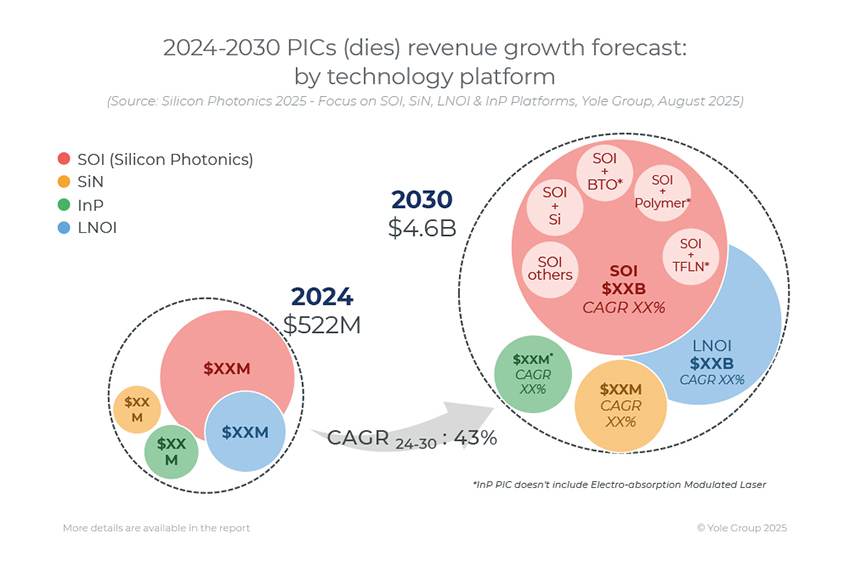
According to data from market research firms, the global silicon photonics market is projected to surge from $278 million in 2024 to $2.7 billion by 2030, achieving a remarkable compound annual growth rate (CAGR) of 46%. This growth trajectory indicates a nearly tenfold expansion in just six years.
The rapid advancement of silicon photonics technology is primarily attributed to the exponential growth in bandwidth demand from AI networks and the urgent need for high-speed interconnect solutions in data centers addressing computational challenges.
Market Outlook: AI-Driven Explosive Growth
The 46% CAGR from 2024 to 2030 underscores the explosive momentum in this sector. This growth rhythm aligns closely with the expansion pace of AI computing demand. The integration density of silicon photonics continues to increase, and its application fields are steadily broadening. The global silicon photonics module market is expected to reach $5.71 billion by 2029, with a projected CAGR of 35.2% in the coming years.
Technical Advantages: The Key to Breaking Bottlenecks
The high expectations placed on silicon photonics technology stem from its unique advantages. Silicon photonics modules are based on silicon photonic technology, integrating optical chips such as lasers, modulators, detectors, couplers, optical waveguides, and multiplexers/demultiplexers onto a single silicon photonics chip. These are then packaged together with electrical chips like DSP, TIA, and drivers to form the complete module.
Research reports indicate that the core advantages of silicon photonics modules lie in their low cost, low power consumption, and high integration density. The high integration level of silicon-based materials and compatibility with CMOS processes endow these modules with these superior characteristics.
Specifically regarding performance, by using CW light sources to replace lasers like EML in traditional optical modules, saving thermal control components (TEC), and optimizing structural components/PCBs, silicon photonics modules achieve approximately 20% cost savings and nearly 40% power consumption optimization. These performance advantages are particularly crucial in the context of the AI computing demand explosion.
Application Scenarios: From Data Centers to a Diverse Ecosystem
The application prospects for silicon photonics are broad and diverse. Data centers and telecommunications networks are the two traditional application scenarios for silicon photonics, but the rise of AI is altering the market landscape. Silicon photonics plays a key role in meeting AI and machine learning demands within data centers, as traditional processor architectures approach physical limits. The high-speed communication enabled by silicon photonics is essential for supporting faster computations.
Beyond traditional fields, silicon photonics shows significant potential in emerging areas. Photonic integrated circuits, particularly Silicon-on-Insulator (SOI) and Lithium Niobate on Insulator (LNOI) platforms, offer versatile solutions for applications requiring massive scalability. Optical LiDAR, 3D integration, quantum computing, optical gyroscopes, and even medical photonics hold notable potentialSensor, though some applications still face technical and regulatory challenges.
Industry Chain Landscape: Global Competition
The silicon photonics industry chain has formed a complete structure comprising "upstream foundational support – midstream manufacturing core – downstream application expansion."
In the upstream segment, high-quality silicon-based materials, advanced lithography equipment, and specialized EDA software form the technical foundation for silicon photonics chip R&D.
The midstream chip manufacturing, packaging, and testing phases directly determine the performance metrics, production yield, and cost-control capabilities of silicon photonics chips.
Downstream system integrators combine silicon photonics chips with other electronic components to develop end products like optical communication modules and optical computing systems for various scenarios. A synergistic effect within the global silicon photonics industry chain is beginning to emerge.
The entire industrial ecosystem is forming around diverse participants, including startups/design houses, research institutions, foundries, and equipment suppliers, collectively driving significant growth and diversification.
Future Trends: Silicon Photonics 2.0 and CPO Technology
The industry believes the global silicon photonics sector has entered its 2.0 phase. In Phase 1.0, the optical communication industry focused on comparing EML lasers and discrete devices against silicon photonic integration technology. The industry extensively validated silicon photonics for optical module applications in terms of bandwidth modulation performance upgrades, monolithic reliability, and cost-effectiveness.
Co-Packaged Optics (CPO) is considered a major future driver for silicon photonics technology. Predictions indicate the CPO market will explode from $46 million in 2024 to $8.1 billion in 2030, with a staggering CAGR of 137%.
Global wafer manufacturing giants are actively deploying silicon photonics chip foundry businesses. They have launched their respective silicon photonics platforms and plan to achieve volume production with more advanced processes in 2025-2026.
As the demand for low-energy consumption, low-latency, and high-density optical interconnects in AI clusters becomes increasingly urgent, silicon photonics technology is no longer merely a future option but an inevitable choice for supporting next-generation digital infrastructure.


 >
>

 >
>
 >
>
 >
>
 >
>
 >
>