TEL:+86 158 1857 3751


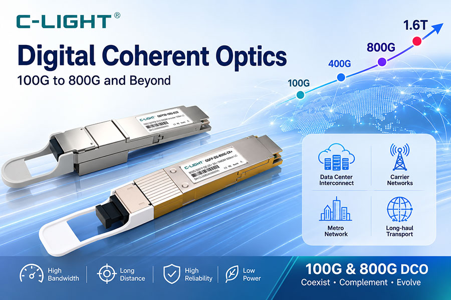
As the core component of full-band OTN networks, ultra-high-speed coherent optical Transceivers directly impact the evolution of optical transmission network infrastructure through their data rate, transmission distance, power consumption, and cost. Currently, 400G long-haul and 800G metro applications have entered the commercial stage, while 800G long-haul and 1.6T metro are in the technology development phase. When the per-channel rate increases, expanding the operating band becomes necessary to support increased fiber transmission capacity. For instance, the operating band for 400G long-haul coherent optical Transceivers is expanding from the C-band to the C+L band. Future T-bit long-haul coherent optical Transceivers will further evolve towards multi-band operation including S, C, and L bands. With the advancement of coherent optical module technology, core components face challenges related to bandwidth, integration, power consumption, and cost, driving innovation and breakthroughs in new materials, architectures, and packaging processes.
Development Status
In the telecommunications sector, CFP2 form factors dominate for long-haul and metro transmission coherent optical Transceivers. For data center interconnects (DCI), QSFP-DD and OSFP are the two main form factors. Standardization, miniaturization, pluggability, and ease of maintenance are traditional requirements for optical Transceivers. The technical status of coherent light sources and optical transceiver components within these Transceivers is described below.
Coherent Light Sources: There are two main technical approaches: integrated lasers and external cavity lasers. Monolithic indium phosphide (InP) integrated lasers cannot achieve C+L band integration. External cavity lasers include two schemes: those using spatial optical filters and those using silicon optical filters. In the spatial optical filter scheme, the wavelength dependency of the high-reflection coating on the etalon makes C+L integration difficult to achieve.
Optical Transceiver Components: The primary materials for coherent optical transceiver components are silicon photonics (SiPh), indium phosphide (InP), and thin-film lithium niobate (TFLN).
Silicon photonics components offer significant cost advantages. They utilize wavelength-agnostic designs, such as adiabatic couplers, supporting C+L integration. However, their modulation bandwidth is limited. A future development direction for SiPh is the integration of TFLN materials to support large-bandwidth modulation.
Indium phosphide components offer large bandwidth but at a higher cost. Their prominent advantage is the ability to integrate semiconductor optical amplifiers (SOAs) for high-power output. Furthermore, wavelength-dependent loss introduced by multimode interferometer (MMI) mixers within the modulator can be compensated by the SOA. However, both the MMI mixers and SOAs in InP chips struggle to support an operating wavelength range exceeding 100nm; consequently, C+L integrated InP devices are not yet commercially available at this stage.
Thin-film lithium niobate, evolved from bulk lithium niobate, supports C+L integration by designing MMIs with minimal wavelength dependency.
Evolution
To support the evolution of optical Transceivers towards ultra-high speeds, technological innovation is required in the electrical interface form factor, optical transceiver components, and device packaging.
Optical Transceivers: Before 2030, pluggable Transceivers will remain mainstream. As the per-lane electrical signal rate on line cards increases to 448 Gbps and beyond, the optical module form factor may evolve in two directions:
Introducing flyover cables to improve electrical signal transmission quality, continuing to support front-panel pluggable Transceivers.
Adopting embedded optical Transceivers within the line card, where the coherent optical module is placed as close as possible to the signal processing chip on the board.
The driving force behind the rate evolution of optical Transceivers is to increase the baud rate and reduce the number of optical/electrical channels to lower the cost per bit. When the symbol rate in the optical domain reaches 400 GBd and above, a dual-wavelength parallel architecture might be adopted to meet higher-rate transmission requirements, considering the cost-performance ratio.
Optical Transceiver Components: Driven by the demand for large bandwidth in optical chips, research on various new material devices has become active, such as those using materials with high electro-optic coefficients like lithium tantalate, barium titanate, lead zirconate titanate, organic polymers, and graphene. The application of new materials in optical components requires demonstrating cost or performance advantages. Using silicon photonics as a platform and integrating other new materials to leverage their respective strengths is an important technological development direction. Heterogeneous integration of SiPh and TFLN is likely to become the mainstream technology for future coherent optical components. This approach supports S+C+L integration and meets the required 400 GBd+ symbol rates around 2030:
Transmitter: SiPh passive components support multi-band operation, while the TFLN waveguide is dedicated solely to modulation, achieving bandwidths exceeding 200 GHz.
Receiver: Thermally tuned phase shifters achieve precise hybrid mixing with a 90° phase difference across multiple bands. Germanium photodetectors support bandwidths above 200 GHz by reducing the photocarrier transit time and optimizing the series resistance.
Device Packaging: The optimization of high-speed signal interconnects between optical chips, electrical chips, and DSP chips is a key driver for the evolution of optical component packaging. Photonic integrated circuits (PICs) will adopt packaging technologies from the integrated circuit industry, such as copper bumps, copper-copper bonding, through-silicon vias (TSVs), integrated capacitors, organic substrates, substrate-like PCBs, and glass substrates. The main difference between PIC packaging and IC packaging lies in the requirement for optical coupling in PICs and the need to protect the optical coupling interfaces during the packaging process. In the near to mid-term, a potential packaging architecture involves using the optical chip as an interposer. The modulator driver and transimpedance amplifier (TIA) chips are flip-chip mounted on top of the optical chip. High-speed interface signals are interconnected with the electrical chips through vias in the optical chip. Copper-copper bonding or bump soldering is used between the optical and electrical chips to achieve short transmission paths and minimize parasitic effects. The DSP chip and the optoelectronic chips are packaged on a common substrate.
Coherent optical Transceivers are developing towards higher bandwidth, higher integration, higher reliability, lower power consumption, and lower cost, driving continuous innovation in core components regarding chip materials, architectural schemes, and packaging processes. Looking ahead, T-bit level optical components are expected to utilize heterogeneous integration of silicon photonics and thin-film lithium niobate to achieve S+C+L integration, supporting high symbol rates of 256 GBd / 400 GBd and beyond.
 >
>

 >
>
 >
>
 >
>
 >
>
 >
>